Samsung Patents a Pixel That Bounces Light Back Instead of Letting It Escape
Samsung is patenting a pixel design that essentially bounces light back through the sensor's detector instead of letting it escape — a way to squeeze more signal out of the same amount of incoming light.
What Samsung's light-bouncing pixel design actually does
Imagine shining a flashlight through a window and most of the light just passes straight through without doing anything useful. That's roughly what happens inside a standard image sensor: light enters, the detector catches some of it, but a portion slips past without being recorded. Samsung's patent addresses that waste.
The design adds two thin layers around the photodiode — the tiny component that converts light into an electrical signal. A special optical layer on the front slightly tweaks the phase of the light (think of it like adjusting the timing of a wave), and a reflective layer on the back acts like a mirror, bouncing uncaptured light back for a second chance at being detected.
The result is that the same pixel captures more light without physically getting bigger. This is especially useful for near-infrared light, the invisible wavelengths used in Face ID-style sensors, night-vision cameras, and depth-sensing systems.
How the phase-shift layer and mirror work together
The patent describes a redesigned image sensor pixel built around three main additions to a standard photodiode:
- An optical phase-modifying layer on the front (light-receiving) side. This thin film has a lower refractive index than the photodiode material itself, which causes a so-called unidirectional π phase shift — essentially a half-wavelength timing flip — specifically tuned to near-infrared wavelengths. That shift is what makes reflected light constructively interfere (reinforce itself) inside the detector rather than cancel out.
- A passivation layer sandwiched between the phase-modifying layer and the photodiode. Passivation layers are standard in chip manufacturing — they protect the semiconductor surface from contamination and electrical defects.
- A reflective layer on the back side of the photodiode. The patent allows this to be a simple metal mirror, a thin-film stack, or a Distributed Bragg Reflector (a precisely engineered multilayer mirror that reflects only specific wavelengths very efficiently).
The combined effect is a resonant cavity: light that passes through the photodiode without being absorbed hits the back mirror, bounces forward, gets phase-adjusted by the front layer, and constructively reinforces itself on the next pass — giving the detector multiple chances to absorb each photon. The patent also references metasurfaces (ultra-thin engineered surfaces that control light at the nanoscale) as a potential variation on the same concept.
What this means for low-light and infrared photography
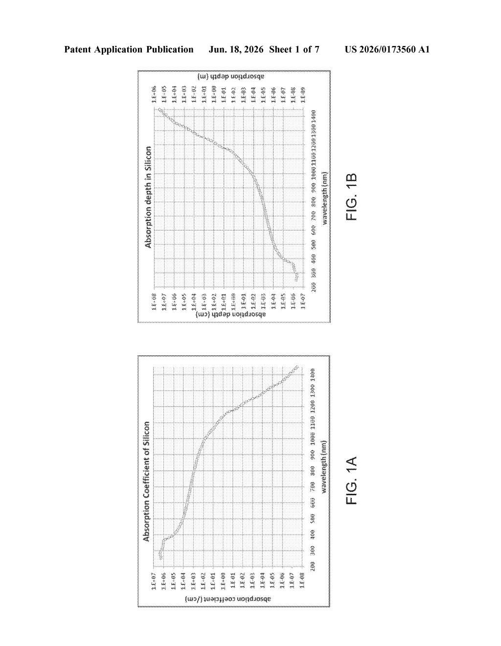
Near-infrared sensitivity is becoming increasingly important in smartphone and wearable cameras. Face unlock, gesture recognition, heart-rate sensors, and LiDAR-style depth mapping all depend on capturing infrared light accurately. Silicon — the standard material for image sensors — is naturally inefficient at absorbing near-infrared wavelengths, which means manufacturers either accept lower performance or use thicker, more expensive sensor materials.
Samsung's approach is an on-chip optical fix: no exotic materials, just carefully engineered thin films added during normal chip fabrication. If it works as described, future Samsung sensors could deliver better low-light and infrared performance without increasing sensor size or cost. That has obvious implications for Galaxy phone cameras and any device using Samsung's ISOCELL sensor family.
This is solid, focused engineering work — the kind of optical physics trick that quietly improves a real product constraint rather than chasing a headline feature. Near-infrared performance is a genuine bottleneck for silicon sensors, and a passive on-chip solution is more manufacturable than switching to germanium or III-V semiconductors. Worth watching when Samsung's next ISOCELL generation lands.
Get one Big Tech patent every Sunday
Plain English, intelligent commentary, no hype. Free.
Editorial commentary on a publicly published patent application. Not legal advice.