Sony Patents a Press-Fit Grounding System for Camera Electronics
Sony has filed a patent for a camera body construction where the physical act of snapping the case shut automatically grounds the internal circuit boards — no separate wiring needed.
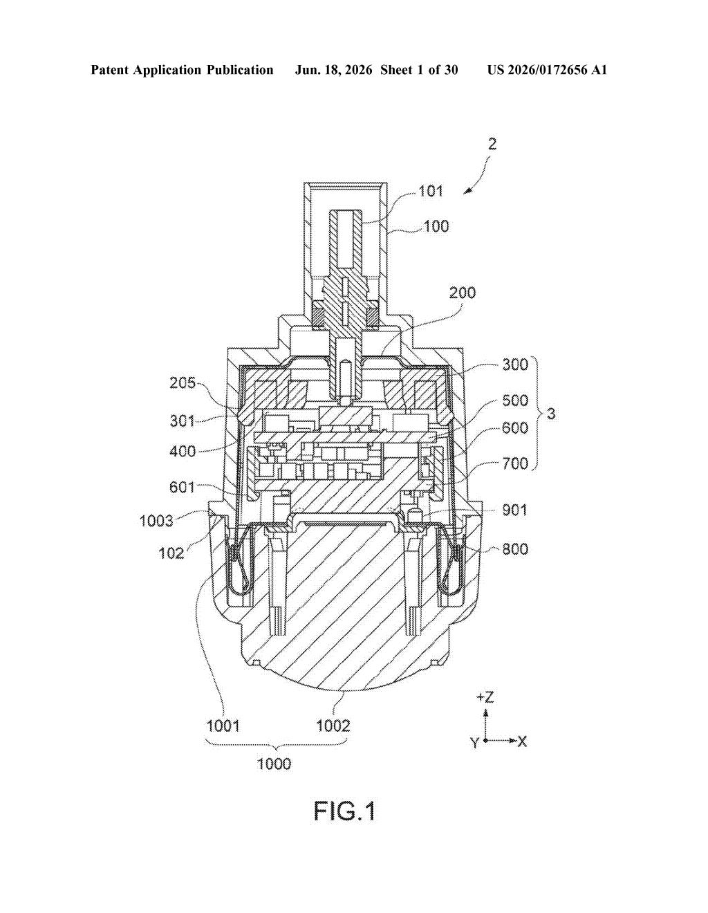
What Sony's press-fit metal chassis actually does
Imagine the circuit boards inside a camera floating loose inside a plastic shell, with nothing to stop stray electrical signals from bouncing around and causing interference. That's a real engineering headache in compact electronics, and it usually requires extra screws, solder points, or grounding wires to solve.
Sony's idea here is to skip those extra steps entirely. The patent describes a metal inner frame — the kind that holds the camera's circuit boards — designed so that when you close the camera's outer shell, the shell's inner walls physically squeeze against the frame's side panels. That pressure alone creates an electrical connection, grounding everything together without any additional fasteners.
A second metal frame sandwiches the assembly from the other side, and the two halves bond together to lock both frames in place and keep them electrically linked. The result is a self-grounding camera body that comes together as it's assembled.
How the case walls create an electrical ground connection
The patent describes a layered sandwich of metal frames and plastic cases that solve a grounding problem in compact image sensors or cameras.
At the center is a first chassis — a conductive (metal) box that holds the circuit board and its components. This chassis has side walls that stick out in two opposing directions. When the chassis is slid into the first case (think of it as the camera's back shell), the case's inner surfaces press against those side walls from the sides. That physical pressure is enough to make an electrical connection — the side walls are now tied together through the conductive case body.
- The first base portion sits opposite the case's bottom, creating a defined orientation.
- The first case's inner walls squeeze the chassis laterally, grounding the side walls to each other via the case material.
- A second chassis — another conductive plate — sits on the opposite side of the circuit board, facing it from above.
- A second case bonds to the first case at their open faces, clamping both chassis pieces together and keeping them electrically connected.
The key engineering move is using assembly pressure as a grounding mechanism. No extra grounding wires or solder bridges are needed — the geometry of the parts does the work.
What this means for camera interference and build quality
For camera and image sensor designers, electromagnetic interference (EMI) is a constant concern. Ungrounded metal parts inside a camera can act like small antennas, picking up or radiating noise that degrades image quality or disrupts wireless signals. Grounding those parts reliably — especially in tiny, densely packed bodies — usually requires careful manual steps during assembly.
A press-fit approach that grounds everything as the body closes could simplify manufacturing and reduce the number of parts. For Sony's image sensor and camera module business, which supplies components to a wide range of device makers, a more reliable, assembly-friendly grounding method has real production value — even if it's not the kind of feature that shows up in a spec sheet.
This is a manufacturing and EMI-shielding patent, not a features patent — it won't change what a camera can do, but it could make compact camera modules cheaper and more reliable to build at scale. Sony's semiconductor division files a lot of structural patents like this, and they tend to quietly show up in the image sensor modules inside phones and consumer cameras. Worth a passing glance if you follow camera hardware supply chains; easy to skip otherwise.
Get one Big Tech patent every Sunday
Plain English, intelligent commentary, no hype. Free.
Editorial commentary on a publicly published patent application. Not legal advice.