Samsung Patents a Two-Stage Light Detector for Faster Chip-to-Chip Optical Links
Moving data around inside a computer with light instead of electricity is one of the bigger bets in chip design right now. Samsung's latest patent describes a compact light-catching structure that sits at the receiving end of those optical links.
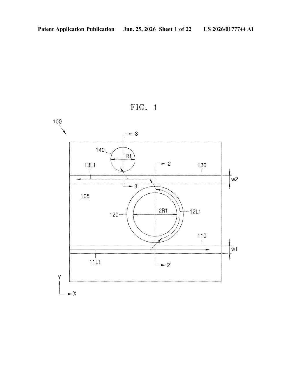
What Samsung's optical light detector actually does
Imagine the wires inside your computer were replaced with beams of light. Data would travel faster and generate less heat, which is a real goal for the next generation of chips. The challenge is that something has to catch that light and turn it back into an electrical signal your processor can use.
Samsung's patent describes a small structure that does exactly that. It uses two resonators, which are tiny loop-shaped or compact curved structures, arranged on either side of a central waveguide (a microscopic channel that guides light). The first resonator is a ring that pulls light in from one waveguide, and the second, smaller resonator on the other side captures what remains and converts it.
The combination of two different resonator shapes is meant to improve how efficiently the device catches light and how well it can be tuned to specific wavelengths. Think of it like a two-stage filter: the first pass grabs most of the signal, and the second catches what might have slipped through.
How the ring and non-ring resonators capture light
The patent describes a light detector structure built for optical interconnects, the technology that sends data as light pulses rather than electrical current inside or between chips.
The structure has four main parts:
- A first waveguide that carries the incoming optical signal (essentially a microscopic light pipe on a chip).
- A second waveguide positioned nearby, which bridges the two resonators.
- A first resonator in a ring shape, sitting between the two waveguides on one side. Ring resonators work by looping light around until a specific wavelength builds up enough to couple into the adjacent waveguide.
- A second resonator on the opposite side of the second waveguide, with a smaller diameter and a non-ring shape. This asymmetry is key: the different geometry means it resonates slightly differently, which can broaden or fine-tune the overall detection bandwidth.
By sandwiching the second waveguide between two resonators of different sizes and shapes, Samsung's design aims to improve light absorption efficiency and signal conversion. The non-ring second resonator is described as the distinguishing element, allowing the structure to handle wavelengths that a single ring-only design might miss.
What this means for optical interconnects in future chips
Optical interconnects are increasingly important as chipmakers look for ways to move more data between processors, memory, and accelerators without the heat and power penalties of copper wiring. A light detector that captures signals more efficiently translates directly into lower power consumption and higher data throughput for the systems using it.
For Samsung, which manufactures both chips and the equipment to build them, this kind of photonics IP is relevant to high-bandwidth memory, AI accelerator packages, and data center hardware. You probably won't notice this component directly, but it could show up in the infrastructure that makes future AI systems faster and less expensive to run.
This is deep infrastructure work, the kind of patent that rarely makes headlines but matters a lot if optical interconnects actually go mainstream in server and AI hardware. The specific contribution, pairing a ring resonator with a smaller non-ring resonator, is a narrow but real engineering choice, not vaporware. Whether it offers enough of an advantage over competing designs to matter commercially is the real question.
Get one Big Tech patent every Sunday
Plain English, intelligent commentary, no hype. Free.
Editorial commentary on a publicly published patent application. Not legal advice.