
Samsung Files Patent for Three-Panel Display System to Enhance VR Headset Clarity
Samsung Display has filed a patent for a headset screen that stitches three separate panels together, putting ultra-sharp displays only where your eyes actually look and using a deliberately textured backing to keep the whole assembly bonded.
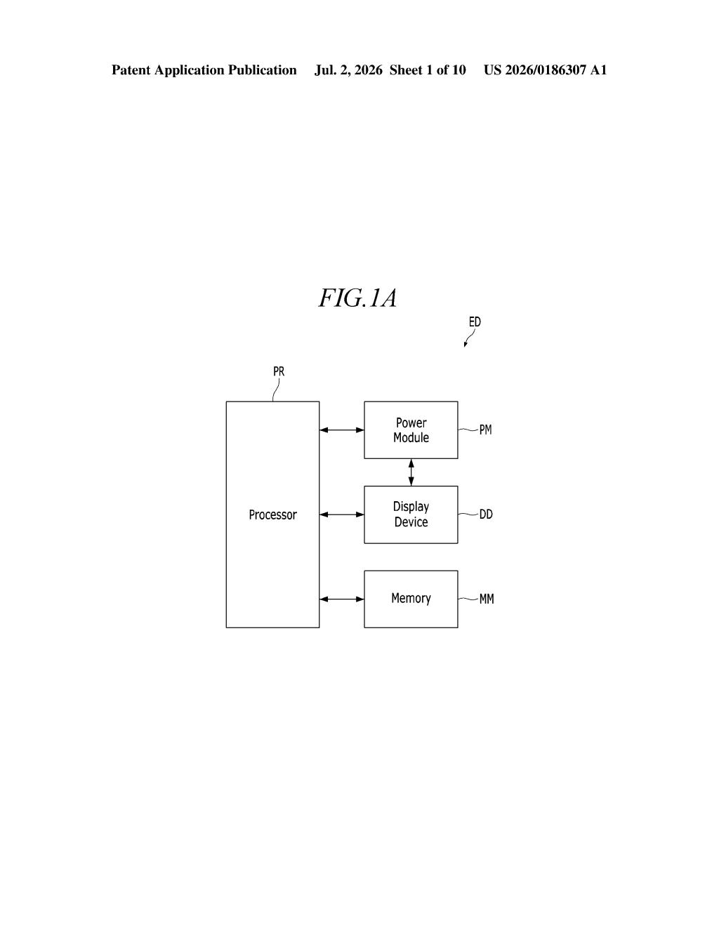
How Samsung's three-panel eye-focus display works
Picture watching a movie through a window. Your eyes naturally focus on the center of the scene, and the edges blur a bit without you noticing. Most VR headsets today use one big flat screen, which wastes a lot of pixels lighting up areas you're barely paying attention to.
Samsung's patent describes a display built from three separate panels. One large panel covers the broad view, and two smaller, much sharper panels sit inside cutouts in the bigger one, positioned right in front of your eyes where detail matters most. Think of it like a high-resolution magnifying glass mounted inside a regular picture frame.
To stop the pieces from shifting or peeling apart, the patent specifies that the areas of the big panel closest to the cutout edges are deliberately roughened at a microscopic level. Rough surfaces grip adhesives and neighboring materials better than smooth ones, so the whole assembly stays together even with heat and pressure over time.
How the panels slot together and why roughness matters
The patent describes a three-panel display stack designed primarily for head-mounted displays (VR and AR headsets). The architecture works like this:
- First display panel: a large substrate (base layer) made from one material, with two holes (openings) cut into its light-emitting layer. This panel handles the peripheral, lower-resolution image.
- Second and third display panels: each made from a different substrate material, they slot into those two holes and deliver higher pixel density (resolution) than the surrounding panel. These sit directly in the line of sight for each eye.
The patent introduces a specific mechanical solution to a bonding problem. The first substrate is divided into two zones: a first region (close to the cutout edge) and a second region (farther away). Samsung specifies that the first region must have a greater surface roughness than the second region. Rougher surfaces at a micro or nano scale create more contact area for adhesives and mechanical interlocking between materials, improving bond strength right where stress concentrates at the panel boundaries.
Using different substrate materials for the high-resolution inserts (likely glass or a rigid crystalline substrate versus the flexible plastic of the outer panel) lets Samsung optimize each panel independently for pixel density, flexibility, or power draw.
What this means for the next wave of VR headsets
VR headsets have long wrestled with a tradeoff: driving an entire high-resolution display at high frame rates is expensive on battery and compute, but a low-resolution display looks grainy where it counts. A foveated hardware approach (putting sharp pixels only where the eye points) is a well-known goal, and this patent shows Samsung Display working on a physical version of that idea without relying entirely on eye-tracking software to redirect rendering.
If this design reaches production, it could mean thinner, lighter headsets with longer battery life than a single full-resolution panel would allow. Given Samsung's partnership with Google on the Android XR platform and its own Galaxy headset ambitions, the timing of this filing is hard to ignore.
This is genuinely interesting display engineering. The rough-surface bonding detail is the kind of unglamorous manufacturing problem that actually decides whether a product ships or stays on a whiteboard. Samsung patenting that specific fix suggests they've hit this failure mode in real prototypes, which means this is closer to production thinking than a pure research exercise.
Get our take in your Top Stories
Liked this breakdown? Add Patentlyze as a preferred source on Google, and our plain-English take shows up more often in your Top Stories the next time Samsung patent news breaks.
There are more where this came from
We read every patent application Big Tech publishes and send you the ones worth knowing. Plain English, free, every week.
Want this weekly breakdown for a company we don't cover? Patentlyze Pro →