
Nvidia Patents a Faster Way to Check and Reshape Chip Circuit Drawings
Designing a modern computer chip means shuffling millions of tiny geometric shapes around a digital canvas, and making sure none of them violate strict spacing rules. Nvidia has filed a patent for a technique that could make that process much faster by describing every shape in terms of distance rather than raw outlines.
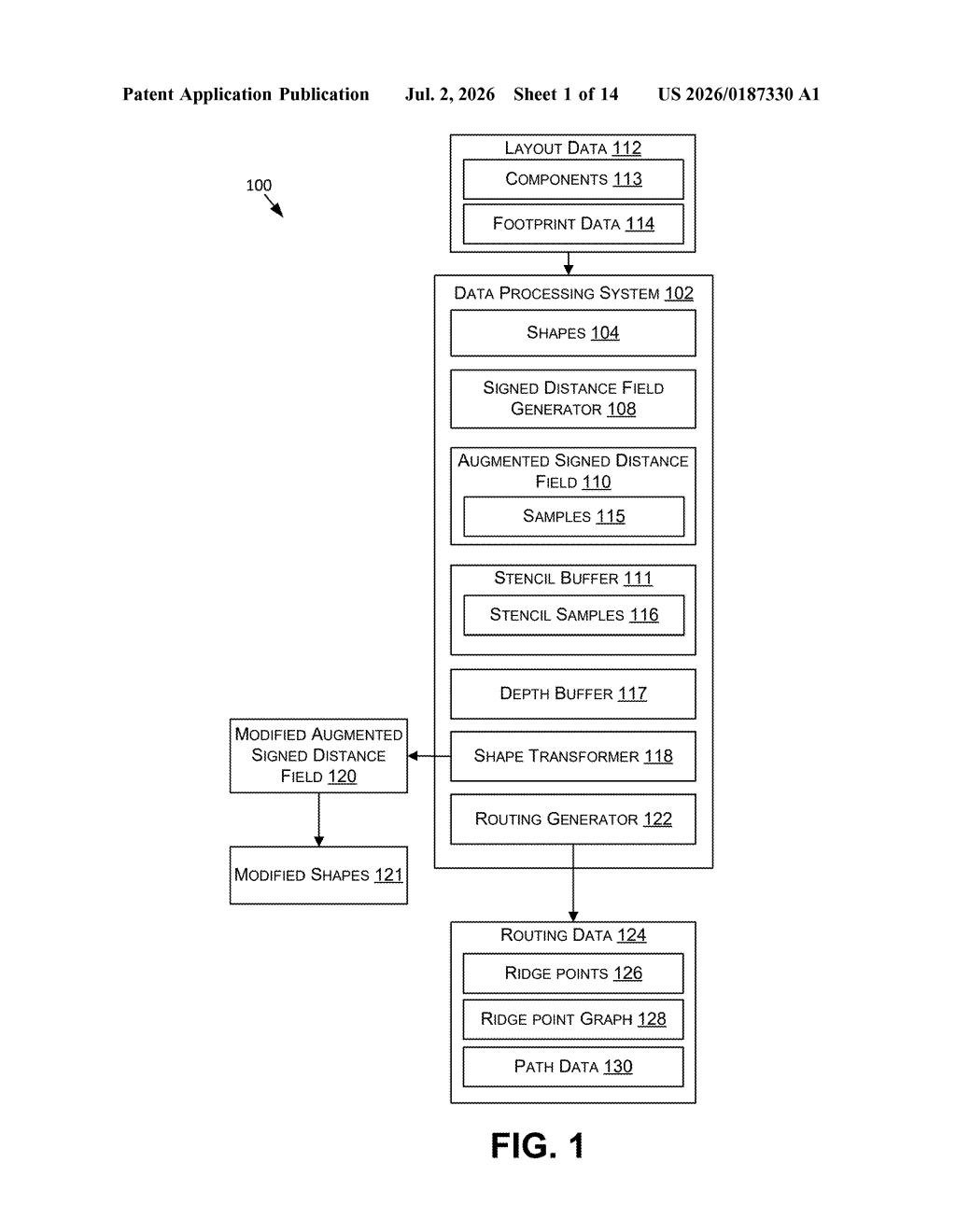
What Nvidia's circuit-layout distance field actually does
Imagine you're laying tile in a bathroom. Before you grout, you need to know exactly how far each tile is from every other tile, and whether you need to trim any edges. Now imagine doing that for a billion microscopic tiles at once. That's roughly what chip designers deal with when they arrange the circuits on a processor.
Nvidia's patent describes a system that converts all those circuit shapes into a special mathematical map called a signed distance field. Instead of tracking each shape's outline point by point, the map stores how far any given spot is from the nearest shape, and which shape it is. Positive numbers mean you're outside a shape; negative numbers mean you're inside one.
With that map in hand, the system can automatically shrink shapes, grow them, or combine them, all without redrawing everything from scratch. It's the kind of back-end geometry work that sounds dull but can shave significant time off the chip design process.
How signed distance fields encode and reshape circuit shapes
The patent covers a system that processes the geometric shapes making up a circuit layout (the blueprint for how transistors, wires, and other components are arranged on a chip) using a technique borrowed from computer graphics called a signed distance field (SDF).
An SDF is a grid where every cell stores two pieces of information: how far that point is from the nearest shape boundary, and a sign indicating whether the point is inside or outside a shape. Nvidia's twist is that each cell also stores an identifier for the closest shape, not just the distance number. That ID tag makes it possible to apply rules that depend on which specific shape is nearby, something a plain distance map can't do.
Using that enriched map, the system can perform three core operations automatically:
- Boolean operations (combining or subtracting shapes from one another)
- Erosion (shrinking shapes inward, to model manufacturing tolerances)
- Dilation (expanding shapes outward, for the same reason)
These operations are a routine but computationally expensive part of design-rule checking, the process of verifying that a chip layout can actually be manufactured without defects. Running them through an SDF representation instead of traditional polygon math can be done in parallel on a GPU, which is Nvidia's core business.
What this means for AI-driven chip design tools
Chip design software is one of the most compute-intensive categories of engineering tools. Every time a designer moves a component or tweaks a wire, the system has to re-verify that thousands of spacing and sizing rules are still met. Techniques that let GPUs accelerate that verification directly shrink the feedback loop between design and sign-off, which matters a lot when a single chip design cycle can cost hundreds of millions of dollars.
This patent fits into a broader industry push toward AI-assisted chip design, sometimes called "EDA" (electronic design automation). If Nvidia can run layout checks faster on its own GPUs, that strengthens the case for using Nvidia hardware in design workflows, including workflows that compete with established EDA vendors like Synopsys and Cadence.
This is genuine infrastructure work, not a headline feature. Signed distance fields are a well-established tool in graphics, but applying them to chip layout geometry with shape-identifier tracking is a specific and non-obvious step. Given that Nvidia sells both the chips and increasingly the software used to design chips, a patent in this space has clear strategic value.
Get our take in your Top Stories
Liked this breakdown? Add Patentlyze as a preferred source on Google, and our plain-English take shows up more often in your Top Stories the next time Nvidia patent news breaks.
There are more where this came from
We read every patent application Big Tech publishes and send you the ones worth knowing. Plain English, free, every week.
Want this weekly breakdown for a company we don't cover? Patentlyze Pro →