
Samsung Patents a Pixel Design That Captures Fine Detail in Bright and Dark Scenes
Samsung has patented a pixel circuit that stacks three separate charge-storage stages inside a single camera sensor pixel, a design aimed at capturing a much wider range of light and dark in a single shot.
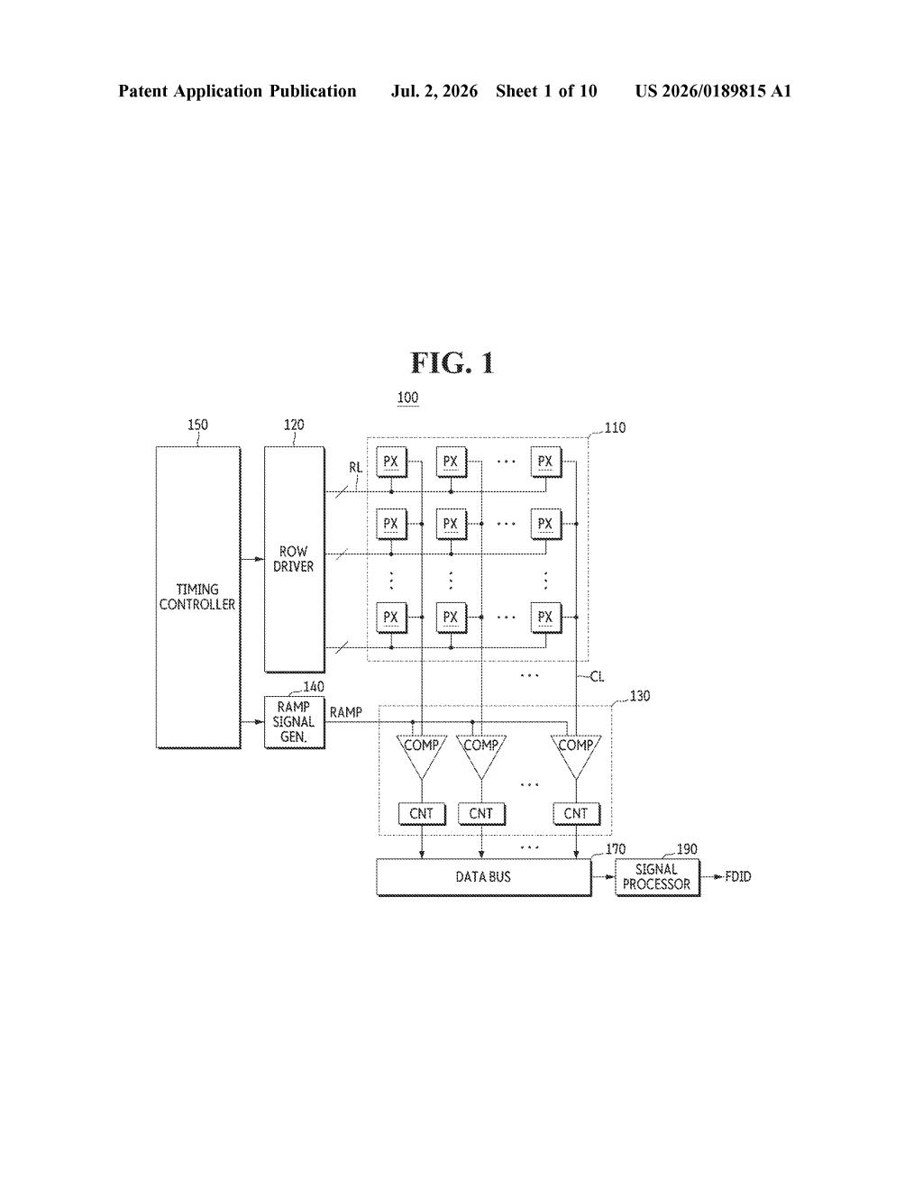
What Samsung's layered pixel design actually captures
Imagine taking a photo on a bright day where the sky is washed out and the shadows are pitch black at the same time. Your camera sensor struggled to hold onto all that information at once. That's the core problem this patent is trying to fix.
Samsung's design gives each tiny pixel in an image sensor three separate "buckets" for storing electrical charge, the signal that light creates when it hits the sensor. Instead of one bucket that overflows in bright light, the system passes charge through a chain of three storage areas, giving the pixel far more room to work with across a wider range of brightness levels.
The result, in theory, is a sensor that holds onto detail in both the brightest highlights and the darkest shadows without needing to take multiple photos and stitch them together. This kind of design is the circuitry-level work that eventually shows up in camera improvements you'd notice in your phone.
How the three floating-diffusion nodes share charge
Each pixel in the sensor contains a photodiode (the part that converts incoming light into electrical charge) and a chain of three floating diffusion (FD) nodes, which are tiny charge-storage points etched into the silicon.
The charge flows through the pixel in stages:
- A transfer transistor moves charge from the photodiode to the first FD node.
- A conversion gain transistor decides whether to pass that charge on to the second FD node, which is connected to a first capacitor (a charge-holding element). This transistor controls how sensitive the pixel is to incoming light.
- A connection transistor then passes charge from the second node to a third FD node, which is connected to a second capacitor wired to the power supply.
- A reset transistor, wired in parallel with that second capacitor, clears the stored charge between frames so the pixel is ready for the next exposure.
The parallel connection between the reset transistor and the second capacitor is the structurally notable detail in the claim. It means the reset path and the storage path share the same voltage reference, which can affect how cleanly the pixel resets and how much residual noise remains before the next shot.
What this means for camera sensors in Samsung devices
Camera sensor dynamic range, the gap between the brightest and darkest detail a sensor can record simultaneously, is one of the most competitive specs in smartphone photography right now. A pixel architecture with three charge-storage stages can hold more total charge before saturating, which is the circuit-level mechanism behind higher dynamic range without requiring software merging of multiple exposures. That means cleaner images from a single capture, especially in mixed-lighting scenes.
Samsung makes its own image sensors (sold under the ISOCELL brand) and supplies them to its own Galaxy phones as well as other manufacturers. A design change at the pixel level like this one would ripple through any product line that uses those sensors, though patents like this frequently describe architectural options rather than shipping designs.
This is deep semiconductor plumbing work, not a flashy announcement. But pixel-level circuit architecture is exactly where camera quality gets won or lost, and Samsung's ISOCELL team files these kinds of patents when they're actively exploring design directions. It's worth tracking as a signal of where Samsung's sensor roadmap is heading, even if this specific layout never ships verbatim.
Get our take in your Top Stories
Liked this breakdown? Add Patentlyze as a preferred source on Google, and our plain-English take shows up more often in your Top Stories the next time Samsung patent news breaks.
There are more where this came from
We read every patent application Big Tech publishes and send you the ones worth knowing. Plain English, free, every week.
Want this weekly breakdown for a company we don't cover? Patentlyze Pro →