
Nvidia Patents an AI System for Auto-Routing Wires Inside Chip Designs
Designing the wiring inside a modern chip is one of the most tedious and error-prone steps in the entire semiconductor process. Nvidia wants to hand a big chunk of that work to an AI that reads the available space mathematically and traces its own paths.
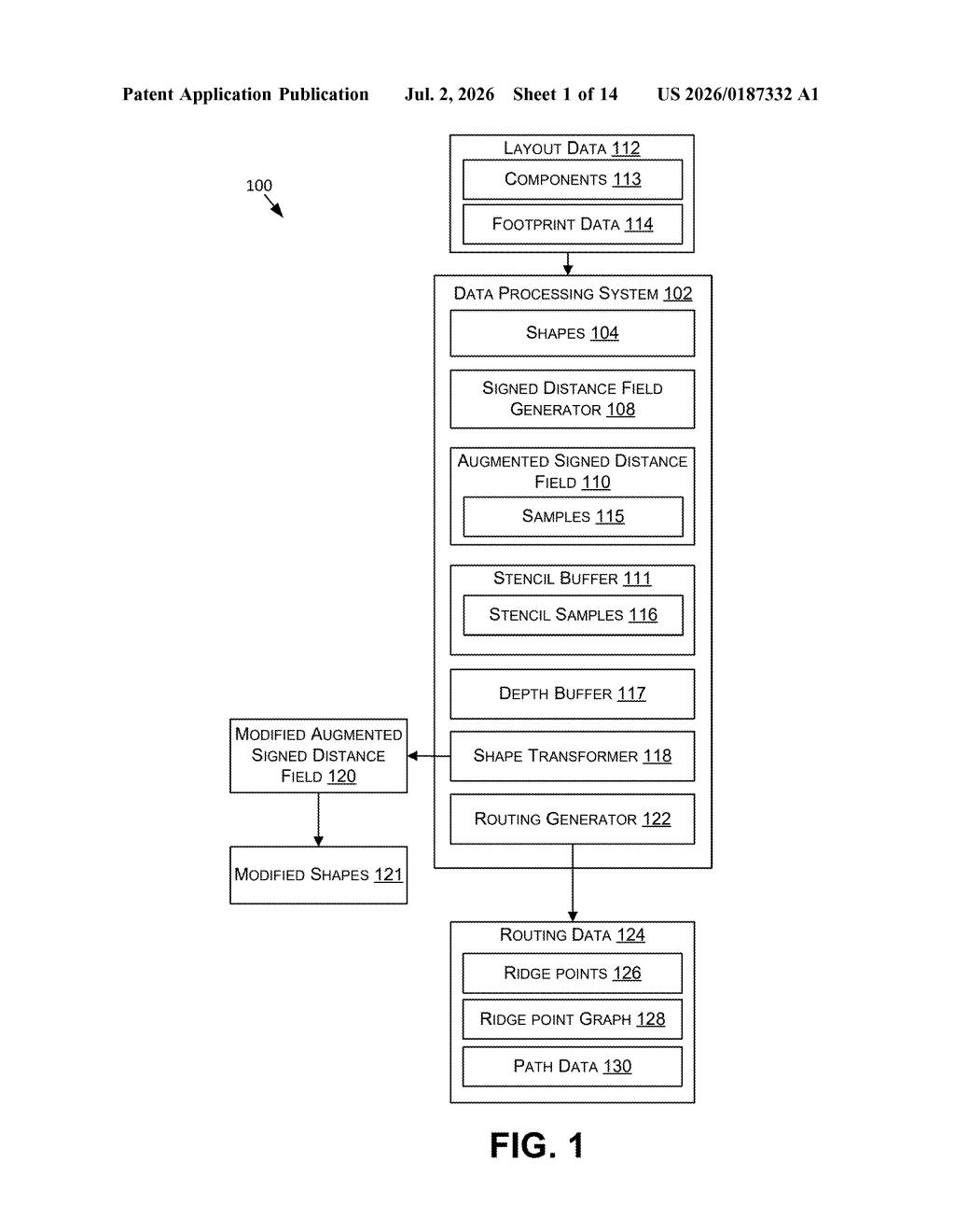
How Nvidia wants to automate chip wiring decisions
Picture a city planner who needs to lay out new roads between buildings, but the buildings keep shifting and the planner has to avoid walls, other roads, and tiny gaps too small for a car. That's roughly the challenge of routing wires inside a computer chip, where millions of connections need to fit in a space the size of a thumbnail.
Nvidia's patent describes a system that treats the empty space on a chip layout like a 3D terrain map. Instead of a human (or a rule-based program) manually guessing where wires should go, the system calculates a distance field, essentially a heat map showing how far every point on the chip is from the nearest obstacle. It then traces the "ridge lines" of that map, the paths that stay as far from obstructions as possible, and turns those into a route the wire can safely follow.
The result is an automated path-finder for chip wiring that could make circuit design faster and less reliant on expert engineers doing repetitive layout work by hand.
How the distance field finds and maps routing paths
The patent centers on a concept called a signed distance field (SDF). An SDF assigns every point in a 2D or 3D space a number representing how far that point is from the nearest boundary or obstacle, positive if you're in open space, negative if you're inside an obstacle. This technique is common in computer graphics (it's how many font renderers and collision engines work), but Nvidia is applying it to chip circuit layouts.
For each sampled point in the chip's layout space, the system also calculates the gradient of the SDF (the direction in which distance changes fastest, essentially a compass arrow pointing away from the nearest obstacle). By analyzing those gradient arrows, the system can find ridge points, locations where the arrows from multiple directions converge, meaning you're equidistant from two or more nearby obstacles at once. Those ridges are the natural center lines of any available routing corridor.
The ridge points are then assembled into a graph data structure (a web of connected nodes and edges, like a road network). Path-planning algorithms can then traverse this graph to find a valid wire route from one point on the chip to another.
- Sample the chip layout as a signed distance field
- Compute gradients at each sample to find ridge lines
- Build a graph of ridge-point nodes
- Run a path-finding algorithm over the graph to produce a routable wire path
What this means for chip design bottlenecks
Chip design is an enormous bottleneck in the semiconductor industry. The physical layout stage, where engineers specify exactly where every wire and component sits, can take months and requires specialized software and expert designers. Tools that automate even a portion of that work can meaningfully shrink the time and cost of producing a new chip.
Nvidia designs some of the most complex chips in the world, including its own GPUs and the AI accelerators that power data centers. A faster, more automated routing system would directly benefit its internal design pipeline. This patent also fits a broader industry trend toward AI-assisted electronic design automation (EDA), where machine learning and geometry-based methods are starting to replace or augment the manual rules that have governed chip layout tools for decades.
This is a technically interesting application of a graphics-world technique to a chip-design problem, and it's the kind of incremental-but-real tooling improvement that compounds over time in a company's internal design process. It's not a product announcement and it won't make headlines outside EDA circles, but for anyone watching the AI-assisted chip design space, it's a concrete signal that Nvidia is investing in automating its own layout pipeline.
Get our take in your Top Stories
Liked this breakdown? Add Patentlyze as a preferred source on Google, and our plain-English take shows up more often in your Top Stories the next time Nvidia patent news breaks.
There are more where this came from
We read every patent application Big Tech publishes and send you the ones worth knowing. Plain English, free, every week.
Want this weekly breakdown for a company we don't cover? Patentlyze Pro →