
Samsung Display Patents a Gate Driving Circuit That Feeds Signals Back Between Display Stages
Samsung Display has filed a patent for a gate driving circuit that links consecutive driver stages through a feedback capacitor, a design choice aimed at keeping pixel-row timing more stable inside OLED and LCD panels.
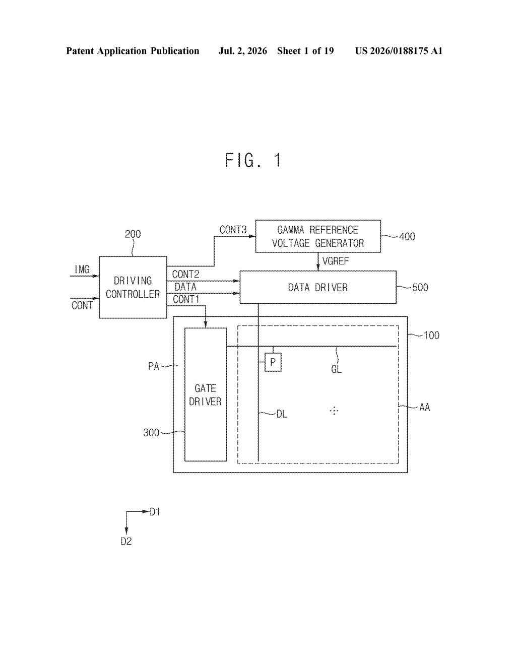
What Samsung's display gate circuit actually does
Every display panel has a hidden circuit that works like a row-by-row starter pistol, telling each line of pixels exactly when to turn on and off. If that timing goes even slightly wrong, you get flicker, ghosting, or uneven brightness.
This patent covers a specific design for that starter-pistol circuit. Samsung's approach adds a small capacitor (essentially a tiny electrical buffer) that feeds a signal from the next row's driver back into the current one. The idea is to keep the voltage at a critical control point stable so the timing stays accurate.
It's a fairly low-level engineering detail, the kind of thing that matters a lot to display engineers but never shows up in a spec sheet. The end result, if it works as intended, is a display that maintains consistent pixel control without needing extra chips or power.
How the feedback capacitor connects the driver stages
The circuit is organized as a chain of stages, where each stage controls one row of pixels on a display. Each stage outputs multiple gate signals (the on/off commands for pixels) that are synchronized to clock signals running through the panel.
The key addition here is a first capacitor that bridges two consecutive stages. One end of this capacitor receives a gate signal from the next stage in the chain. The other end connects to the first control node of the current stage. A control node is simply a point in the circuit whose voltage level determines whether transistors switch on or off.
By tying a downstream signal back to an upstream control point, the capacitor acts as a stabilizer. When the next stage fires, the voltage it produces gets coupled back, helping hold the current stage's control node at a reliable level.
- Multiple gate signals per stage (not just one) let the circuit drive pixels with finer timing resolution.
- The feedback capacitor reduces the risk of voltage drift at the control node between switching events.
- The design keeps additional components inside the panel's existing driver circuit rather than adding external hardware.
What this means for Samsung's display hardware
Gate driving circuits are embedded directly into the glass of most modern OLED and LCD panels, so any improvement to their reliability or power efficiency scales to every display Samsung ships. A more stable control node means less need for compensation circuitry elsewhere, which can simplify the overall panel design.
For consumers, the direct benefit is theoretical at this stage, but circuits like this feed into the engineering baseline for future panels. Displays that maintain tighter pixel timing tend to show less flicker at low brightness, which matters if you use your phone or monitor in dark rooms. It's also the kind of incremental work that adds up across a product generation.
This is a routine display-driver patent and a very narrow one at that. It addresses a real engineering problem (control-node voltage instability in multi-output gate stages), but there's nothing here that signals a product direction or a meaningful departure from standard practice. Worth filing for legal coverage; not worth circling on a product roadmap.
Get our take in your Top Stories
Liked this breakdown? Add Patentlyze as a preferred source on Google, and our plain-English take shows up more often in your Top Stories the next time Samsung patent news breaks.
There are more where this came from
We read every patent application Big Tech publishes and send you the ones worth knowing. Plain English, free, every week.
Want this weekly breakdown for a company we don't cover? Patentlyze Pro →