
Sony Patent Merges Transistor Gates to Boost Image Sensor Performance
Sony is rethinking how the tiny electronic switches inside a camera sensor are built, merging two separate gate controls into one continuous structure that bridges the wall between neighboring pixels.
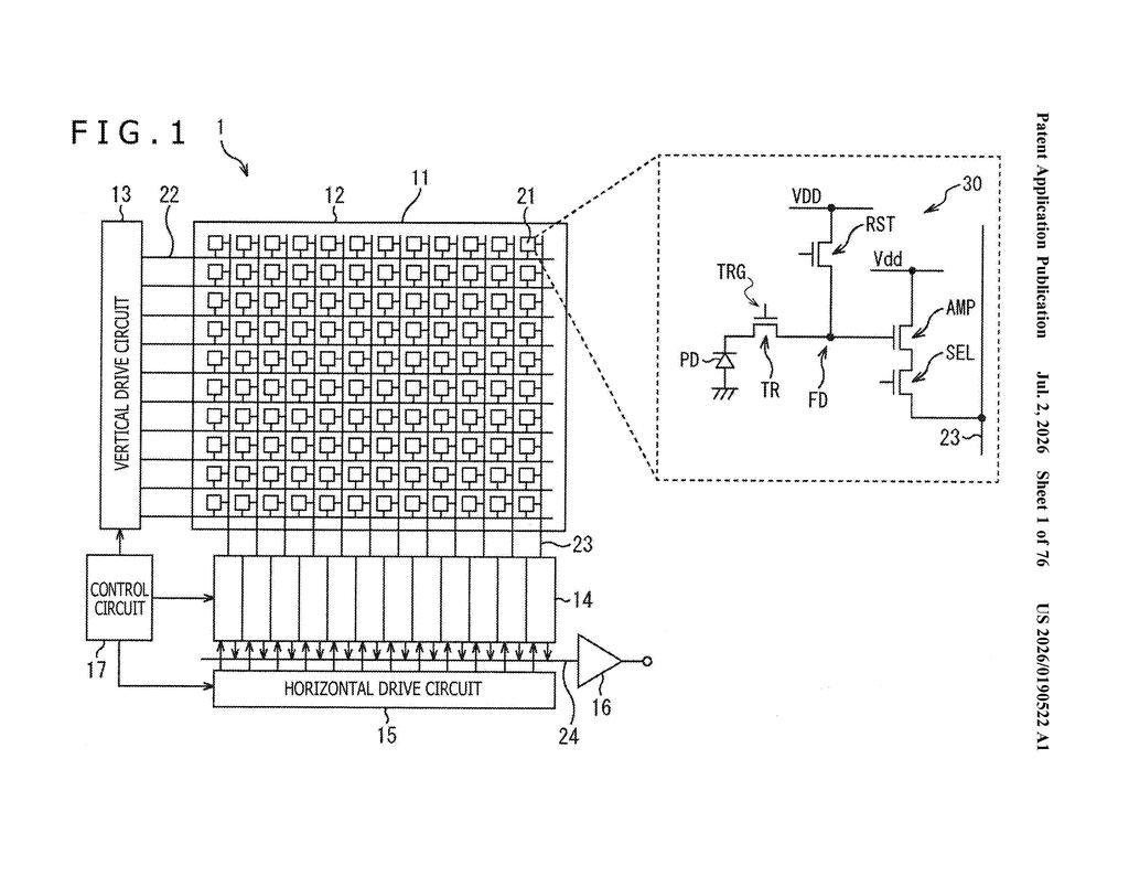
What Sony's pixel-gate design actually does for your camera
Imagine a camera sensor as a grid of tiny buckets, each one collecting light. Between every bucket is a wall that keeps the light from spilling from one bucket into the next. Each bucket also has a small electronic switch that controls when it sends its collected light signal onward for processing.
Right now, each switch sits entirely on its own side of the wall. Sony's patent describes fusing two neighboring switches together at the top, so their control electrode forms one continuous piece that stretches over the wall between them. The idea is that this unified structure reduces electrical imperfections that creep in when two separate electrodes are placed very close together in a tight space.
The practical goal is straightforward: fewer electrical gremlins inside the sensor means cleaner signal handling, which can help preserve image quality as Sony keeps shrinking pixel sizes to fit more of them into the same chip area.
How the integrated gate bridges the inter-pixel barrier
Inside any digital camera sensor, each pixel has a set of pixel transistors that act as gatekeepers, reading out the electrical charge that light has built up and passing it along to the rest of the chip's circuitry.
The patent focuses on two of those transistors that sit on opposite sides of an inter-pixel separating section (the physical barrier etched into the silicon to prevent one pixel's signal from leaking into a neighbor). Normally, each transistor has its own gate electrode, the thin conductive layer that switches the transistor on and off. In this design, the gate electrode of one transistor and the gate electrode of the transistor directly across the barrier are physically merged into a single, continuous electrode that arches over the top of that barrier.
- The two transistors share one unified gate structure instead of sitting under two separate, independent electrodes.
- The merged gate spans the inter-pixel separating section, using the upper portion of that barrier as its bridge.
- Because the structure is continuous rather than two separate pieces crammed close together, it can reduce the kind of electrical interference and manufacturing variability that degrades sensor performance at small scales.
The core claim is about performance preservation: as pixel pitches shrink and transistors get packed closer together, keeping them electrically well-behaved becomes harder, and this architecture is Sony's proposed answer.
What this means for future Sony camera sensors
Camera sensors are in an ongoing arms race to pack more pixels into a smaller area without sacrificing low-light performance or signal accuracy. Every time pixel size shrinks, the transistors controlling each pixel get crowded, and electrical noise or manufacturing imperfections become a bigger problem. Sony's integrated-gate approach is a structural fix aimed squarely at that problem.
Sony Semiconductor Solutions supplies image sensors to a wide range of camera makers, including smartphone vendors. A design that keeps sensor performance stable at smaller pixel sizes could show up in future high-density smartphone and camera chips. That said, this is a foundational semiconductor architecture patent, so the path from filing to shipping product is long and uncertain.
This is a quiet but serious piece of sensor engineering. It won't make headlines on its own, but Sony's semiconductor division files patents like this because pixel scaling genuinely is getting harder, and structural solutions at the transistor level are where real gains come from. If you follow image sensor technology, it's worth bookmarking.
Get our take in your Top Stories
Liked this breakdown? Add Patentlyze as a preferred source on Google, and our plain-English take shows up more often in your Top Stories the next time Sony patent news breaks.
There are more where this came from
We read every patent application Big Tech publishes and send you the ones worth knowing. Plain English, free, every week.
Want this weekly breakdown for a company we don't cover? Patentlyze Pro →