
Qualcomm Patents a Chip Package That Buries Power-Stabilizing Capacitors Closer to the Processor
Every processor needs a steady supply of electricity, and even tiny fluctuations can cause errors or slowdowns. Qualcomm's new patent describes a way to bury power-stabilizing components directly inside the chip package, right next to the processor, to keep that power supply rock-steady.
What Qualcomm's embedded-capacitor chip package actually does
Imagine your phone's processor is a car engine that needs a perfectly smooth fuel supply. Any hiccup in that supply, even a brief one, can cause the engine to stutter. Computer chips face the same problem: when they suddenly demand more power, the electrical supply can dip for a split second, causing errors. Little components called capacitors act like small local fuel tanks, releasing stored charge to fill those gaps instantly.
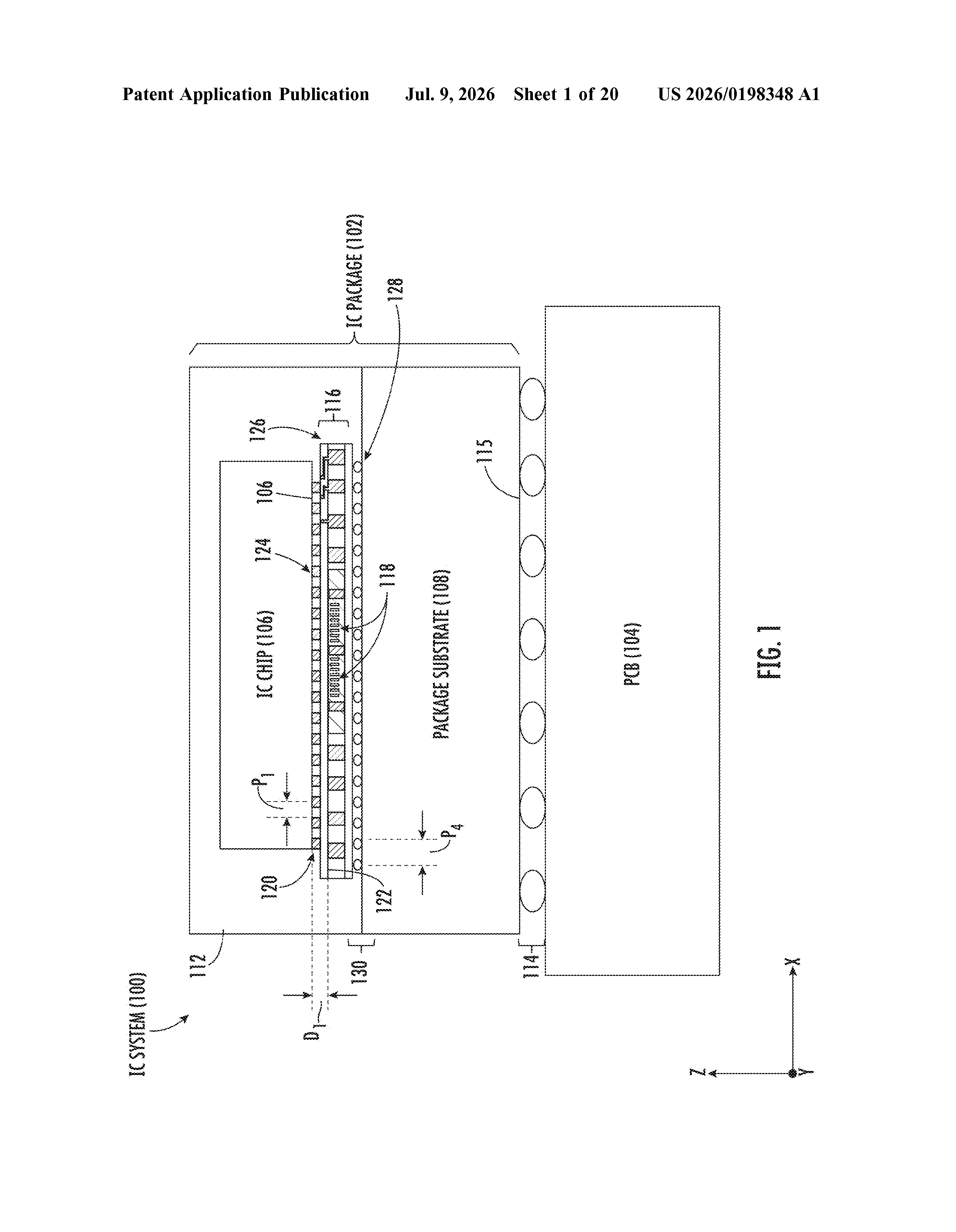
The catch is that capacitors work best when they're physically close to the chip. The farther away they are, the more electrical noise builds up in the connecting wires before the charge arrives. Qualcomm's patent describes a way to embed those capacitors directly inside a thin wiring layer that sits between the main circuit board and the chip itself, getting them as close to the processor as physically possible.
This sandwiched wiring layer, called a redistribution layer, also handles the job of translating between the chip's dense, fine connection points and the broader wiring of the circuit board below. So Qualcomm is solving two problems at once: tighter power delivery and better wiring compatibility for its highest-density chips.
How the RDL substrate sandwiches the capacitor into the power path
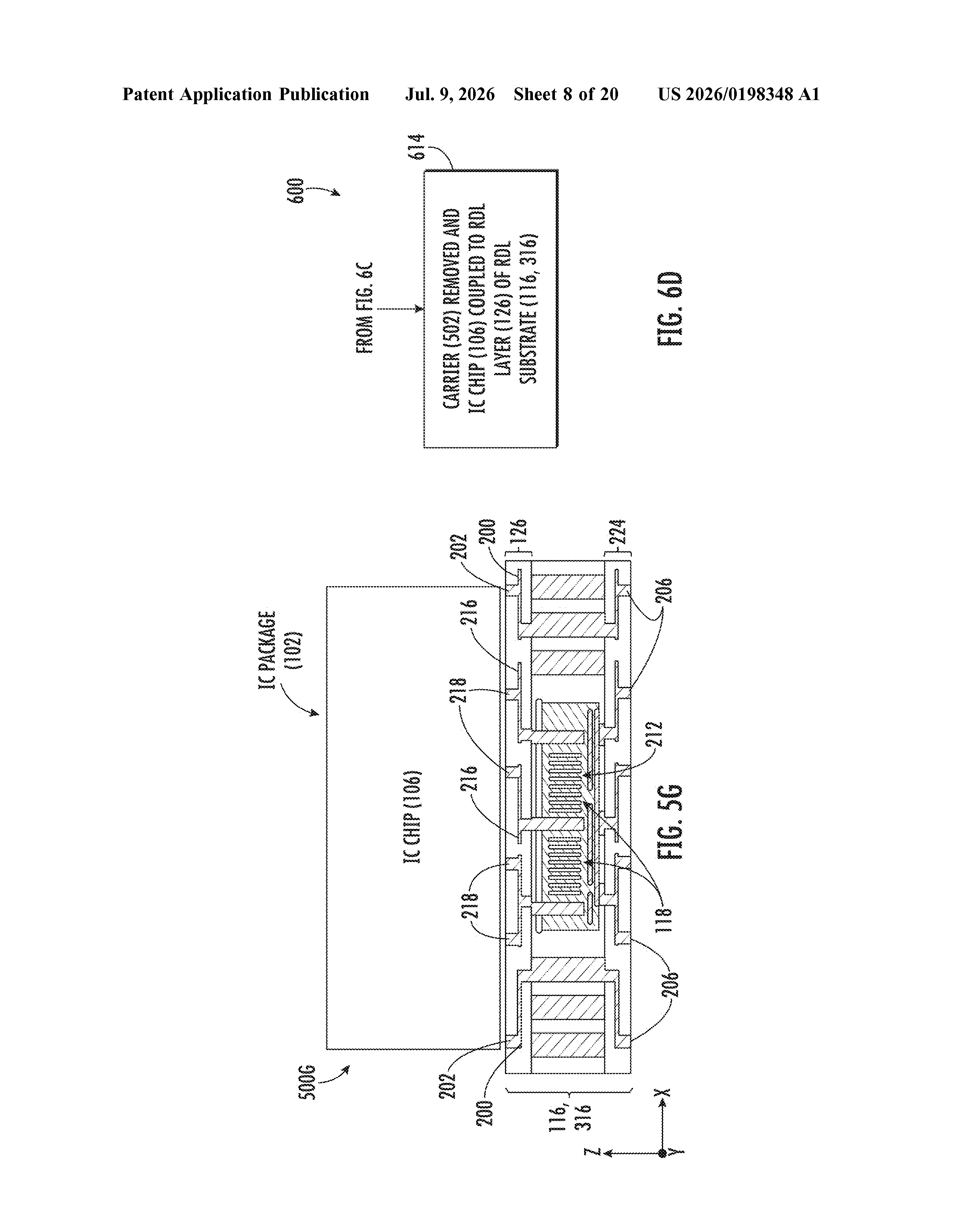
The patent centers on an RDL substrate (redistribution layer substrate), a thin intermediary layer that sits between a processor chip and the main package substrate (the board-like base that everything mounts to).
Normally, decoupling capacitors, the components that smooth out power fluctuations, are placed on the package substrate, which is some distance away from the chip. That distance creates parasitic inductance (unwanted electrical resistance and delay in the wiring), which allows PDN noise (power delivery network noise, meaning tiny voltage spikes and dips) to reach the chip before the capacitor can react.
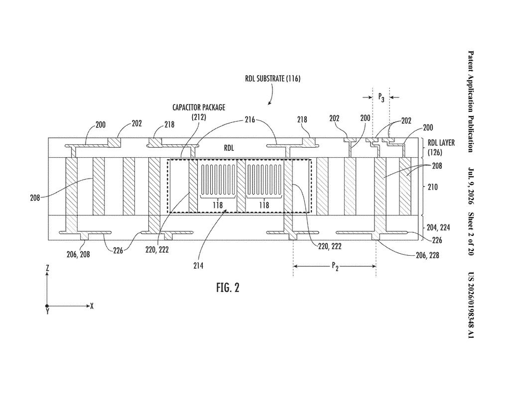
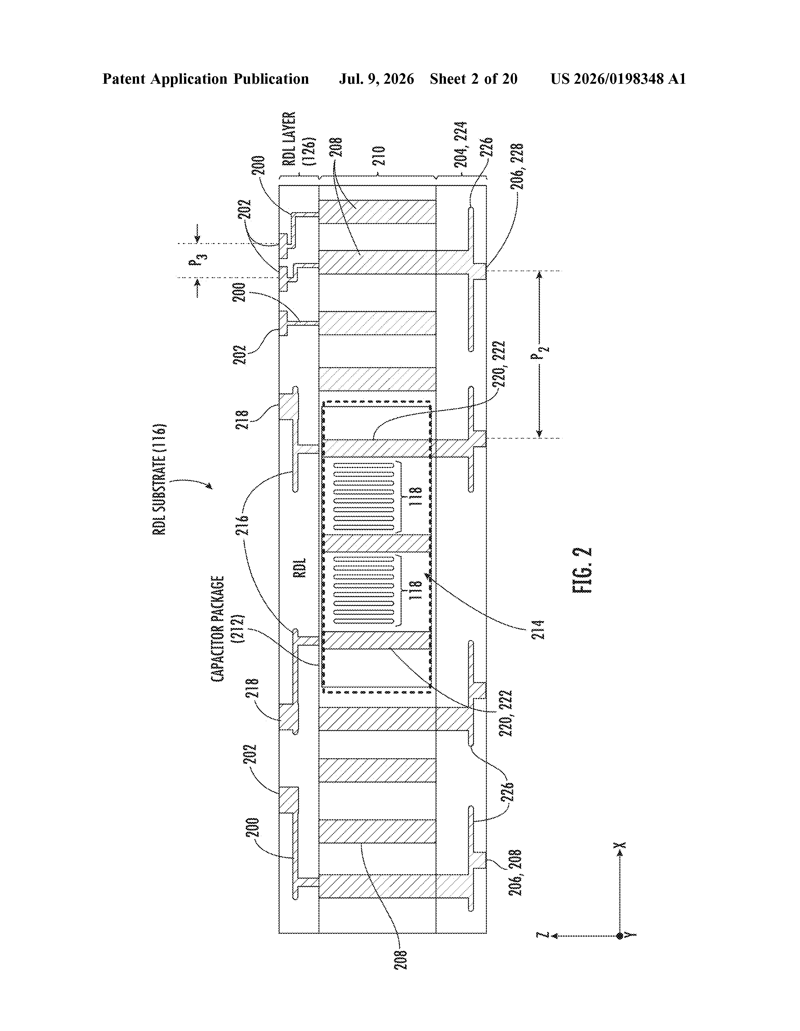
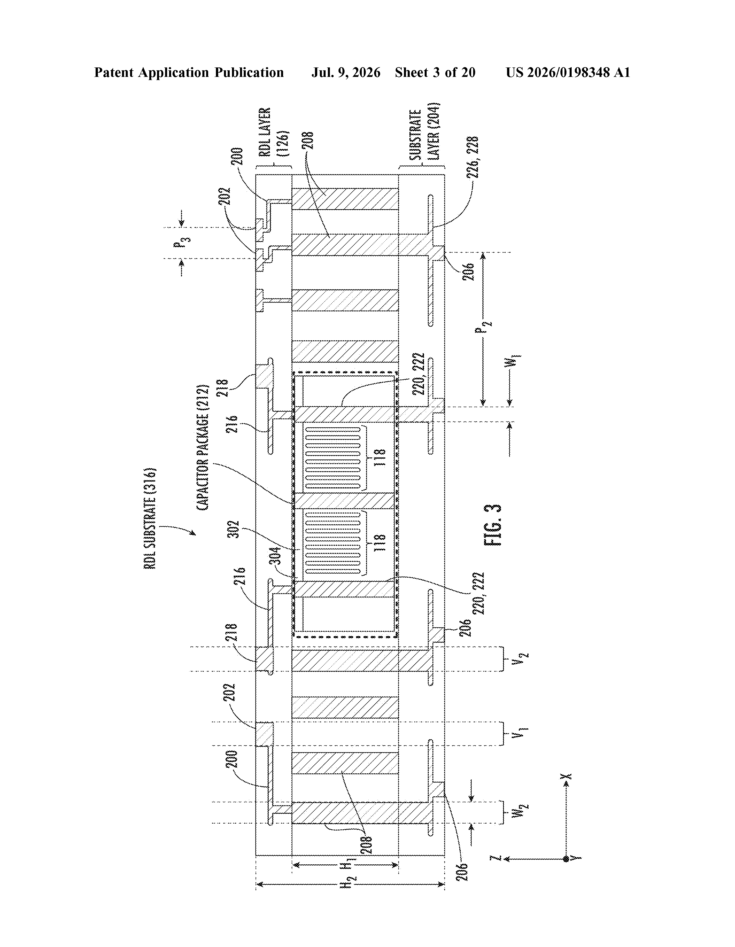
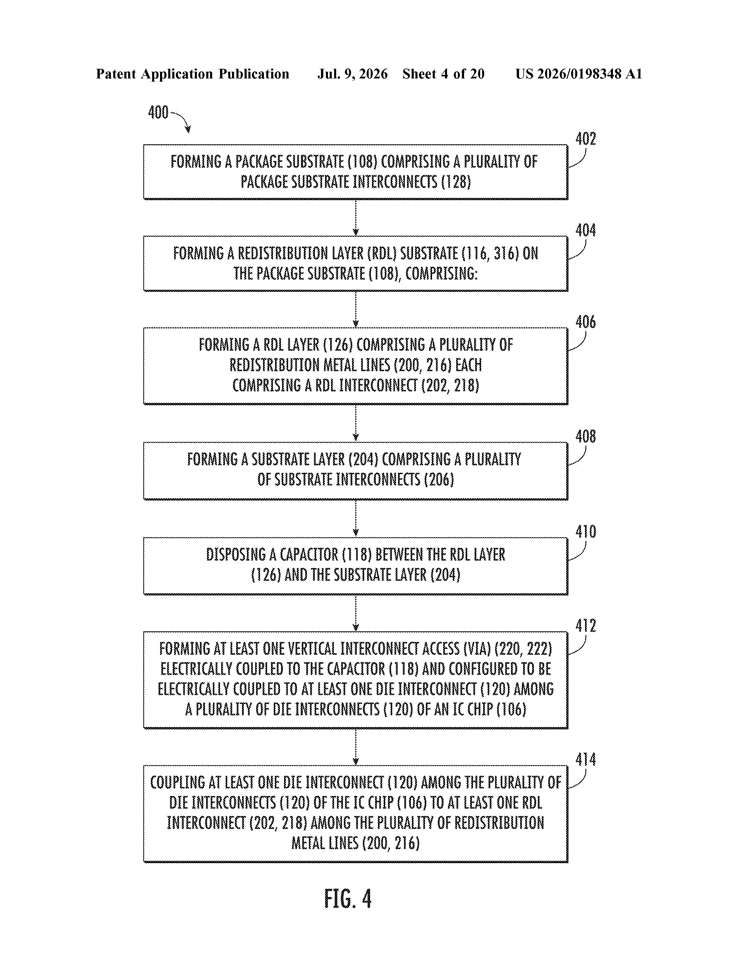
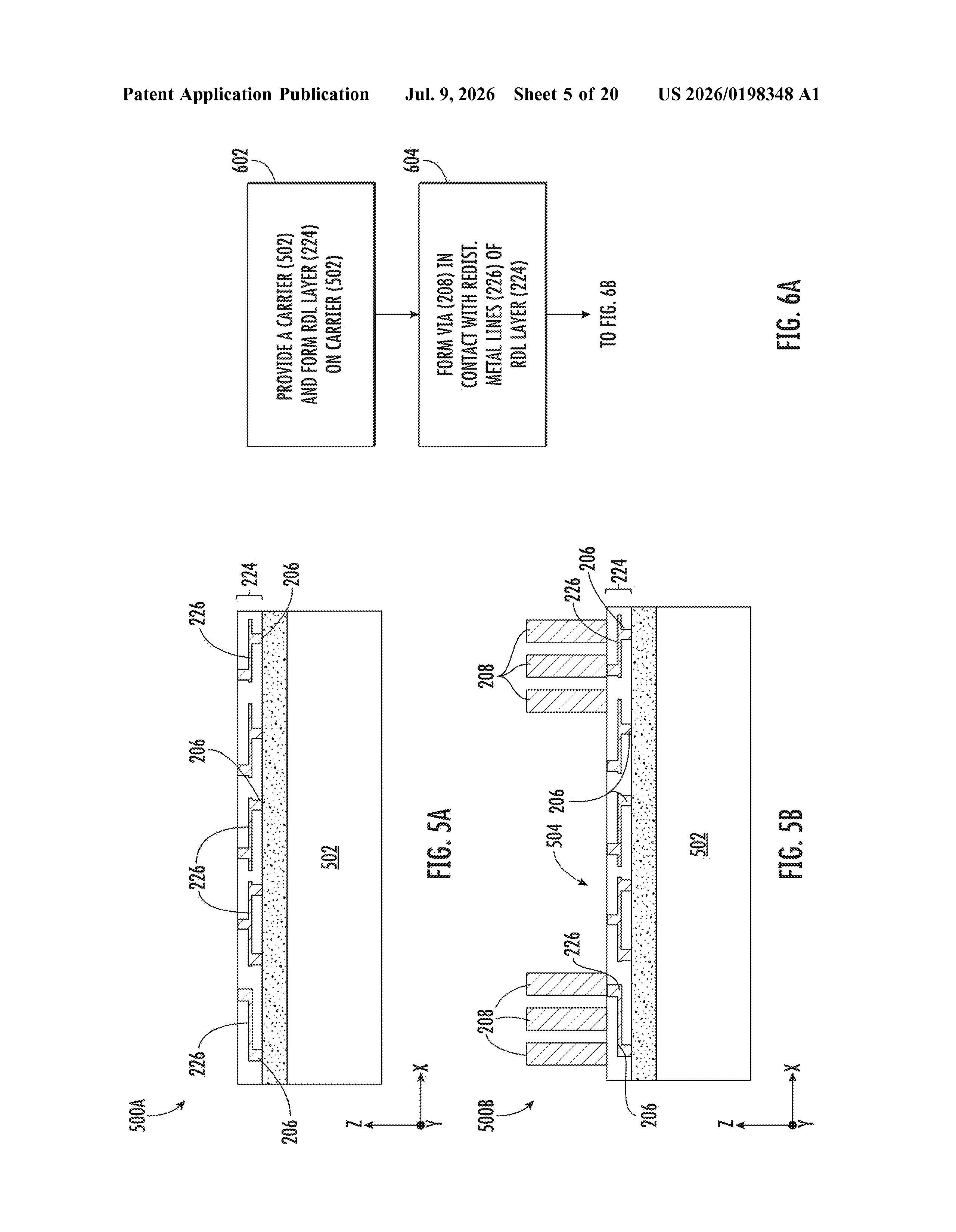
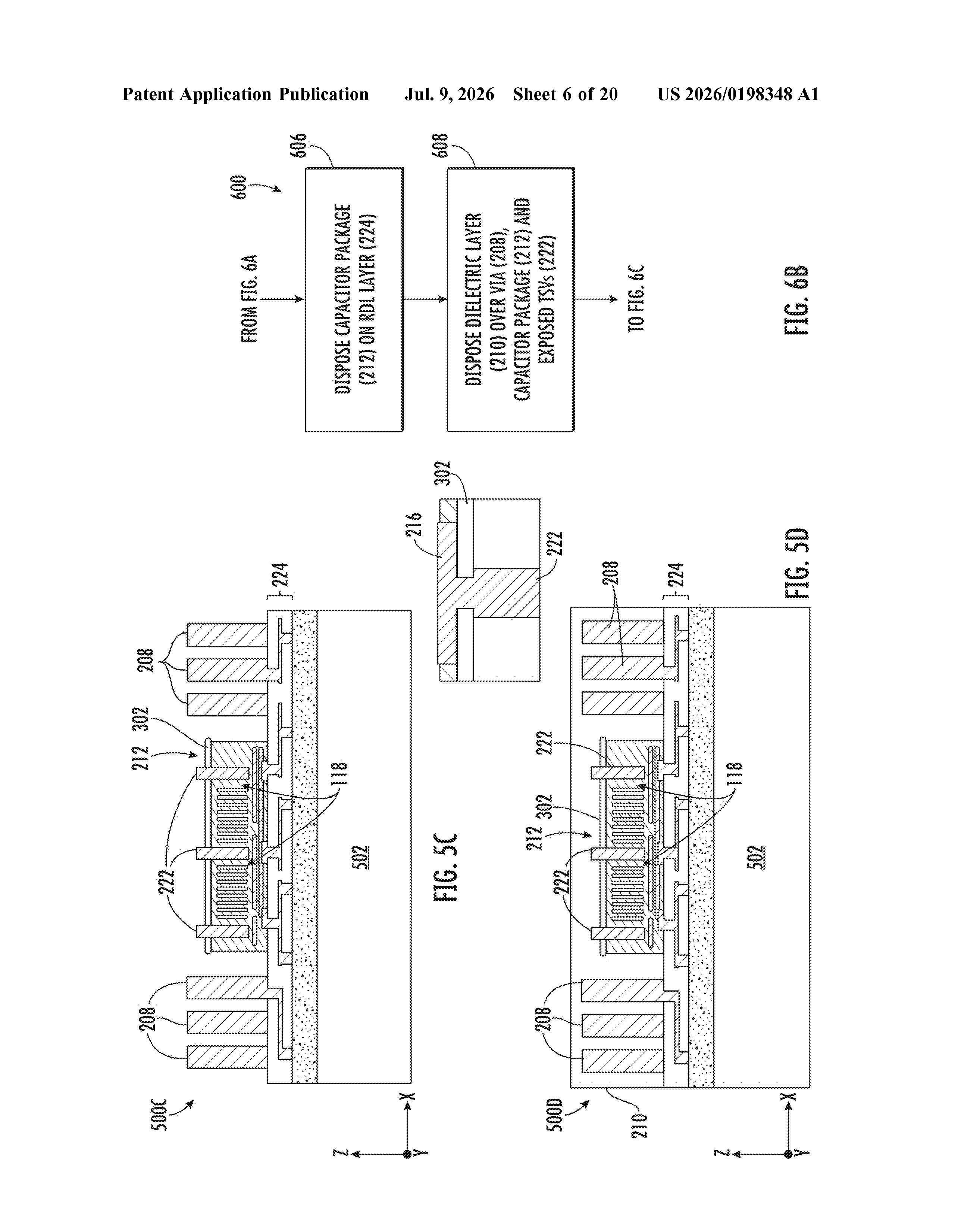
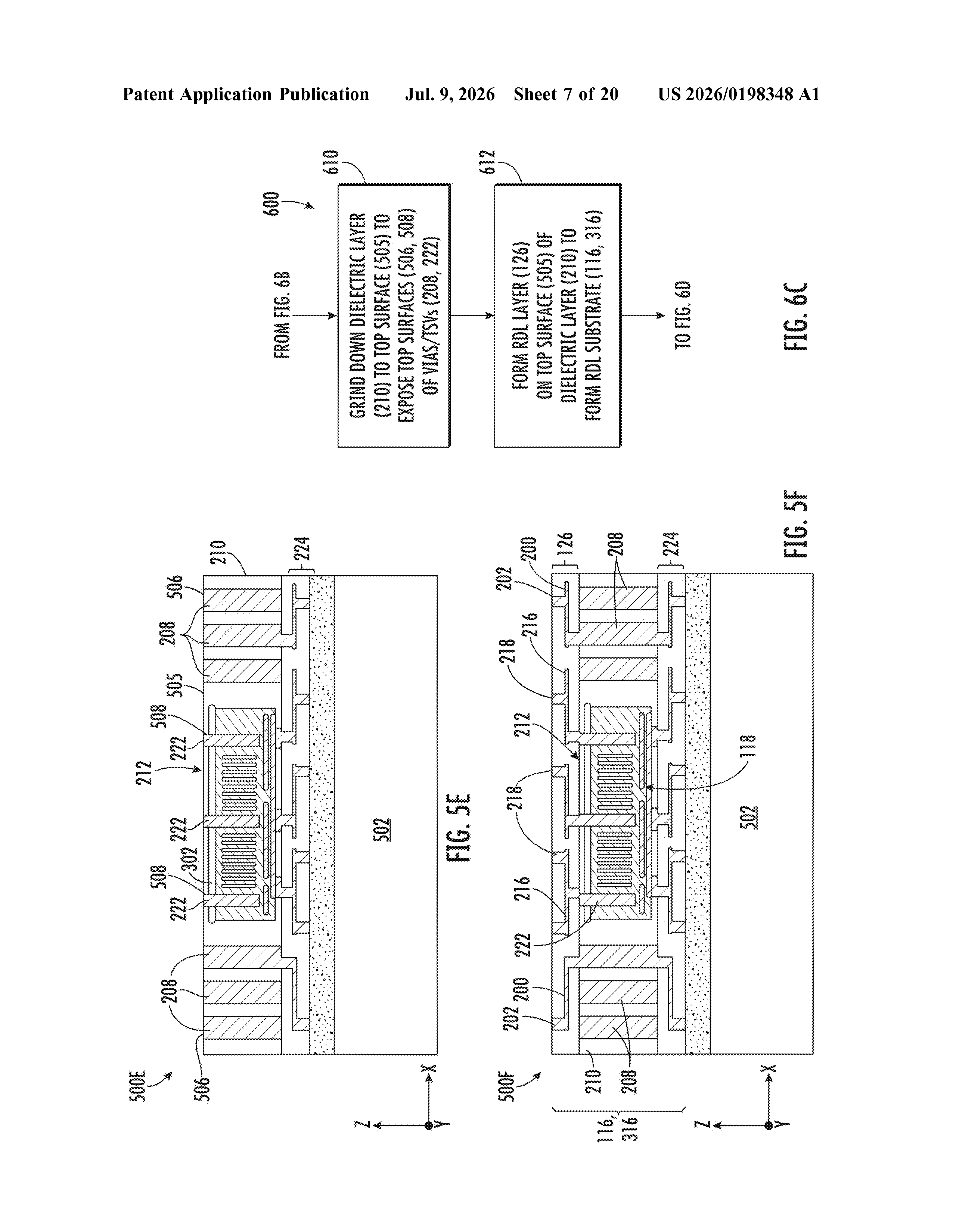
Qualcomm's design embeds the capacitor directly inside this intermediate RDL layer, dramatically shortening the electrical path. Key structural elements include:
- An outer RDL layer facing the chip, with fine-pitch metal interconnects that can match the chip's dense connection grid
- Embedded capacitors within the RDL substrate, oriented vertically so they extend toward both the chip and the package substrate
- Through-vias (vertical electrical channels drilled through the layer) that carry signals between the chip and the main substrate without going around the capacitor
The result is a power supply path where charge storage is physically adjacent to the chip, and signal routing still passes cleanly through the same layer. The design also provides fan-out capability, meaning it can spread the chip's tightly packed connection points out to the wider spacing the package substrate uses.
What this means for chips that need stable power at high speed
For chips running at very high clock speeds, like the processors Qualcomm puts in flagship phones and data-center hardware, even microsecond power dips can trigger errors or force the chip to slow itself down as a safety measure. Getting decoupling capacitors closer to the die is a well-understood goal in chip packaging, and this design offers a concrete structural approach to do it without requiring an entirely new chip architecture.
The fan-out wiring capability built into the same layer is also notable. As chip connection densities keep rising, the gap between what a chip needs and what a standard package substrate can support grows. An intermediate RDL layer that handles both power smoothing and connection translation could become a practical bridge for Qualcomm's high-end mobile and compute chips.
This is unglamorous but genuinely important semiconductor packaging work. Power delivery is one of the real bottlenecks as chips get faster, and embedding capacitors closer to the die is a well-motivated engineering direction. Whether Qualcomm's specific structural approach wins out over competitors' packaging innovations is an open question, but this is the kind of incremental-but-real progress that actually shows up in product performance.
Get our take in your Top Stories
Liked this breakdown? Add Patentlyze as a preferred source on Google, and our plain-English take shows up more often in your Top Stories the next time Qualcomm patent news breaks.
There are more where this came from
We read every patent application Big Tech publishes and send you the ones worth knowing. Plain English, free, every week.
The drawings
20 drawing sheets from US 2026/0198348 A1 · click any drawing to enlarge
Want this weekly breakdown for a company we don't cover? Patentlyze Pro →