
Samsung Patents a Computer Chip That Sends Data Using Light Beams
Samsung is working on a way to package a processor, memory, and an optical data connection all on the same base layer, letting chips talk to the outside world using light instead of copper wires.
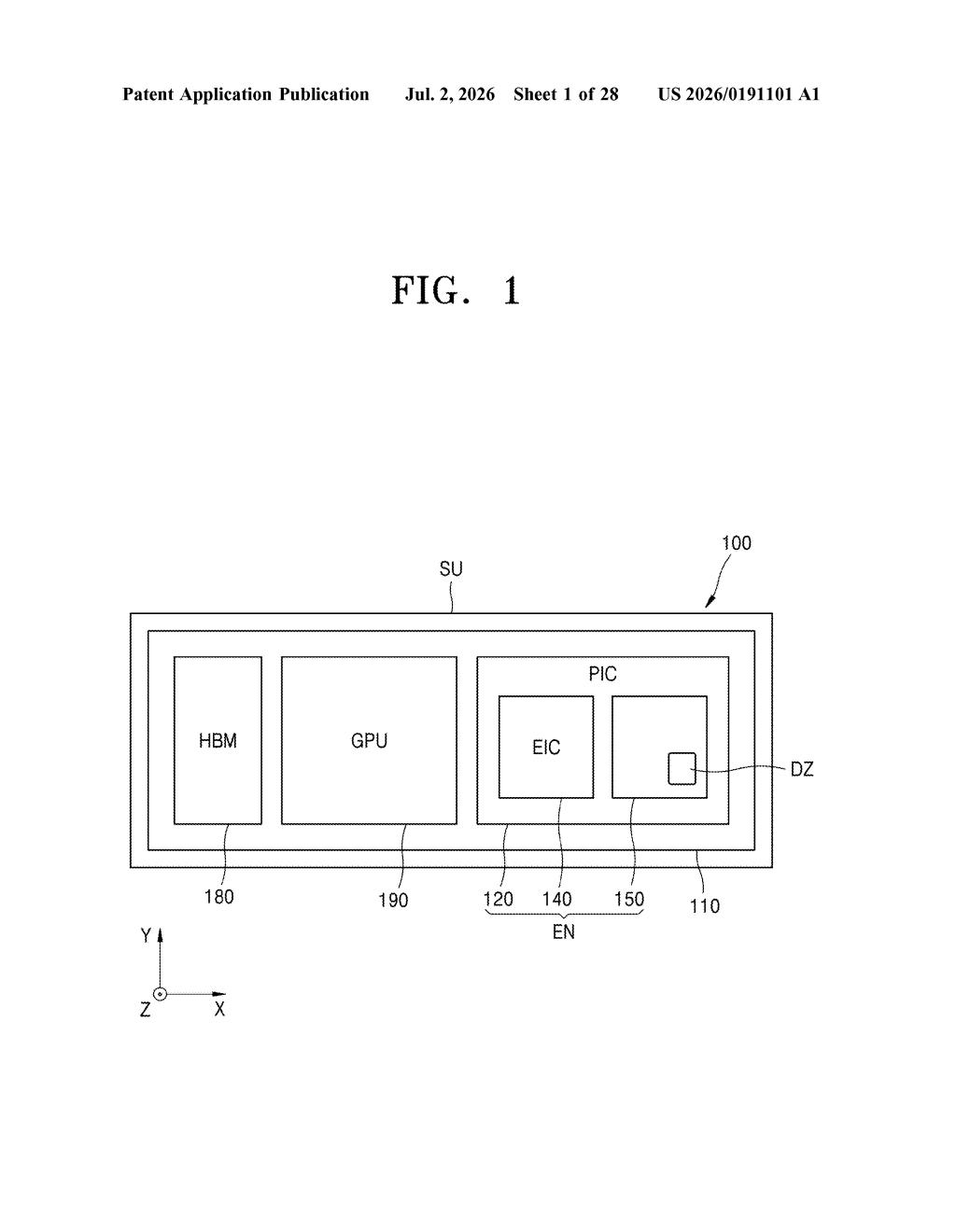
What Samsung's light-based chip package actually does
Imagine your computer's processor and memory sitting on a small platform, and instead of sending data out through metal wires, they fire pulses of light down a fiber-optic path. That's the basic idea here. Samsung's patent describes a chip package that includes an optical engine built right in, alongside the processor and memory, all mounted on a shared base called an interposer.
The tricky part is making the light connection reliable during manufacturing. The patent focuses on a structure that guides light in and out of the chip using a set of tiny patterns. Some of those patterns are "effective" (they actually carry light) and some are "dummy" patterns (they exist only to make the manufacturing process more consistent and protect the real ones during sealing).
The result is a single, compact package that can send and receive data optically without needing a separate external module. That's relevant for AI servers and data centers, where moving massive amounts of data between chips is one of the biggest bottlenecks.
How the optical engine sits inside the processor package
The patent describes a processor package built on an interposer (a thin silicon or glass substrate that acts as a wiring board connecting multiple chips). On that interposer sit three main components: a processor, memory, and an optical engine.
The optical engine contains a photonic integrated circuit (PIC) chip, which converts electrical signals to light and back again (photoelectric conversion). Attached to the PIC chip is a coupling structure that manages how light enters and exits the package.
That coupling structure is where the patent gets specific. It includes:
- An effective pattern that actually receives incoming light from outside the package
- A dummy pattern that does not carry live signals but exists to stabilize the manufacturing process
- A mold layer placed over the dummy pattern, which protects surrounding structures during the encapsulation step of manufacturing
The dummy-plus-mold arrangement is a fabrication technique. When chip packages are sealed in epoxy or resin during production, uneven surfaces can cause stress or cracking. Filling in non-functional areas with dummy patterns and a mold layer keeps the surface geometry consistent, reducing defects in the real optical paths nearby.
What this means for high-speed AI and data center chips
For AI training clusters and high-performance data centers, the connection between chips is increasingly the limiting factor. Electrical copper interconnects consume a lot of power and struggle to keep up with the bandwidth that modern AI chips demand. Integrating optics directly into the processor package, rather than attaching them as a separate pluggable module, can cut latency and power consumption for those inter-chip links.
For everyday consumers, this is far upstream of any product you'd buy soon. But if this kind of co-packaged optical technology matures, it feeds directly into the server infrastructure behind AI services you already use. Samsung competing in this space puts it alongside efforts from Intel, Broadcom, and others to make co-packaged optics a standard feature of next-generation AI accelerator packages.
This is a genuine engineering challenge patent, not a concept sketch. The specific focus on dummy patterns and mold layers to solve optical-coupling manufacturing defects shows real process-level work. Co-packaged optics is a serious research direction for AI infrastructure, and Samsung filing in this area signals it is not leaving that market to US and European chipmakers alone.
Get our take in your Top Stories
Liked this breakdown? Add Patentlyze as a preferred source on Google, and our plain-English take shows up more often in your Top Stories the next time Samsung patent news breaks.
There are more where this came from
We read every patent application Big Tech publishes and send you the ones worth knowing. Plain English, free, every week.
Want this weekly breakdown for a company we don't cover? Patentlyze Pro →