
Samsung Patents a Storage Circuit That Handles AI Calculations Directly On-Chip
Most chips spend more energy moving data than computing with it. Samsung's patent describes a memory cell that skips the trip entirely by doing the math right where the data lives.
What Samsung's computing bit cell actually does
Imagine your computer had to drive to a different building every time it needed to do basic arithmetic. That's roughly what happens inside a traditional chip: data gets stored in memory, then ferried over to a separate processor to be calculated, then sent back. All that back-and-forth burns power and takes time.
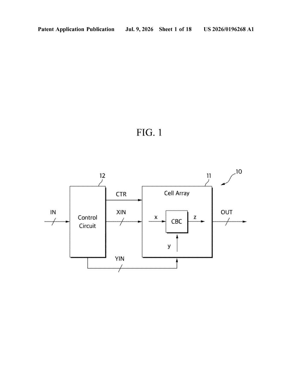
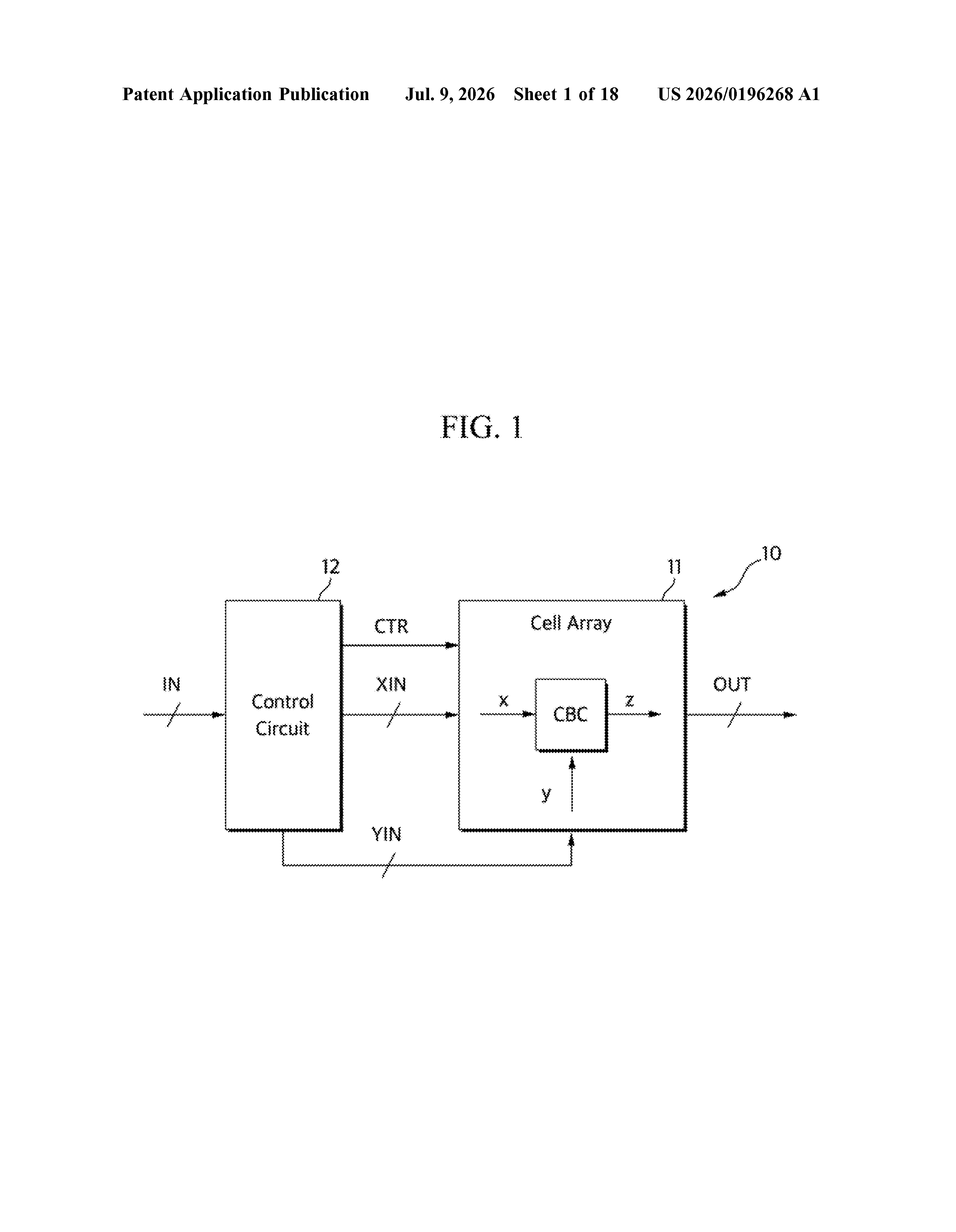
Samsung's patent describes a computing bit cell that breaks that pattern. Instead of just holding a number passively, this tiny memory unit can also perform a multiplication step on its own, using the stored value and two incoming signals. The calculation happens right inside the memory array, no long-distance trip required.
This kind of design is especially useful for AI workloads, which involve multiplying enormous lists of numbers (called weights or coefficients) by incoming data billions of times per second. Doing that math closer to where the numbers live can cut the power bill and speed up results, which matters a lot for things like on-device AI assistants or neural-network accelerator chips.
How three transistors multiply inside the memory array
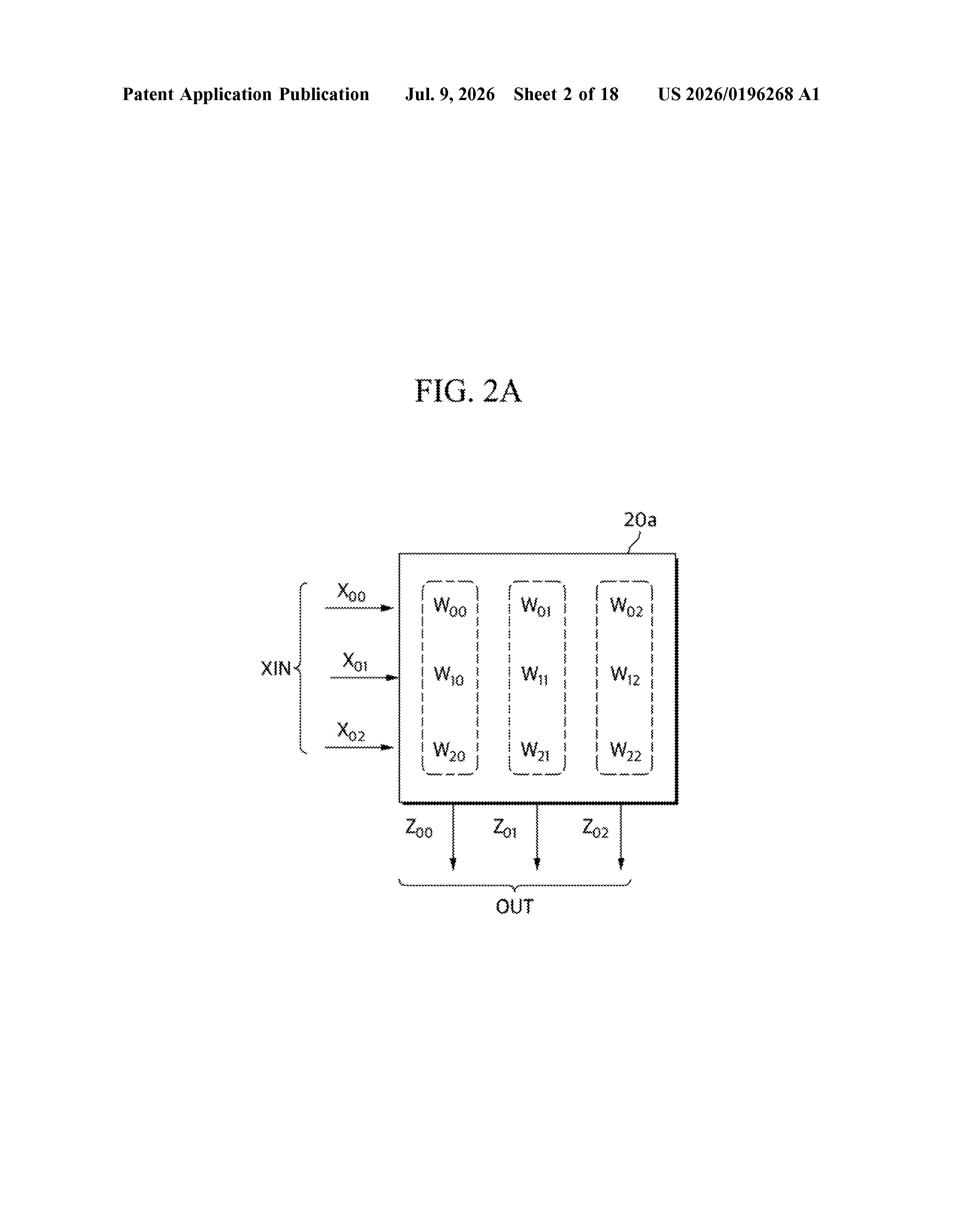
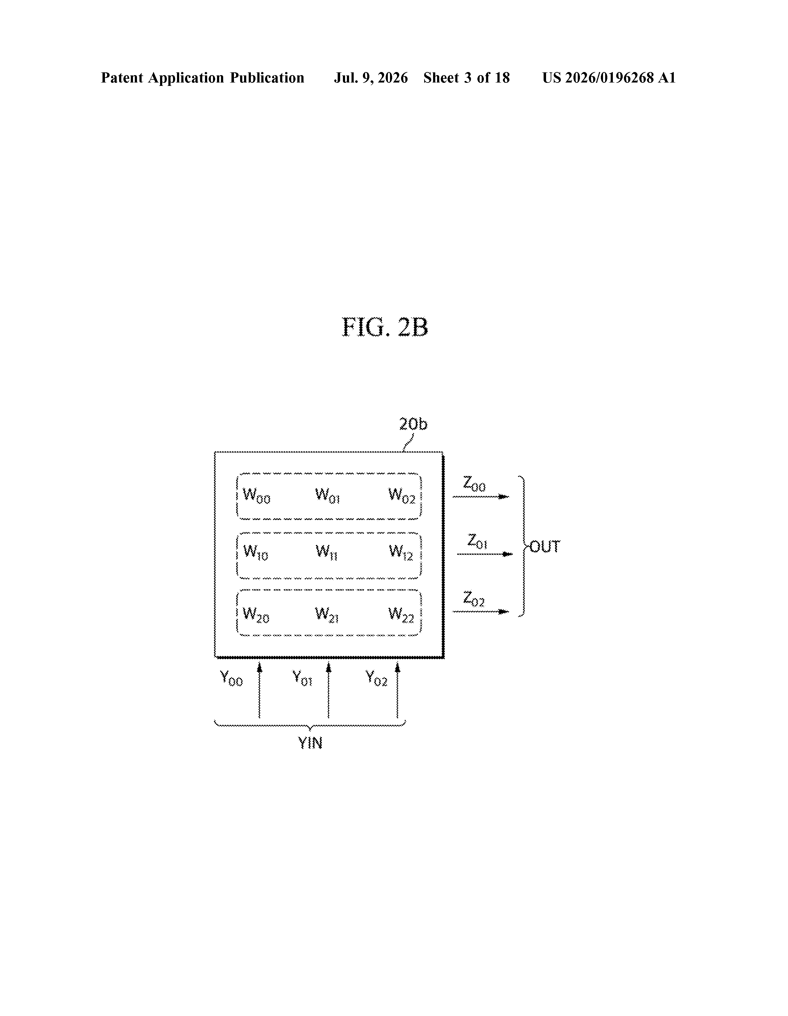
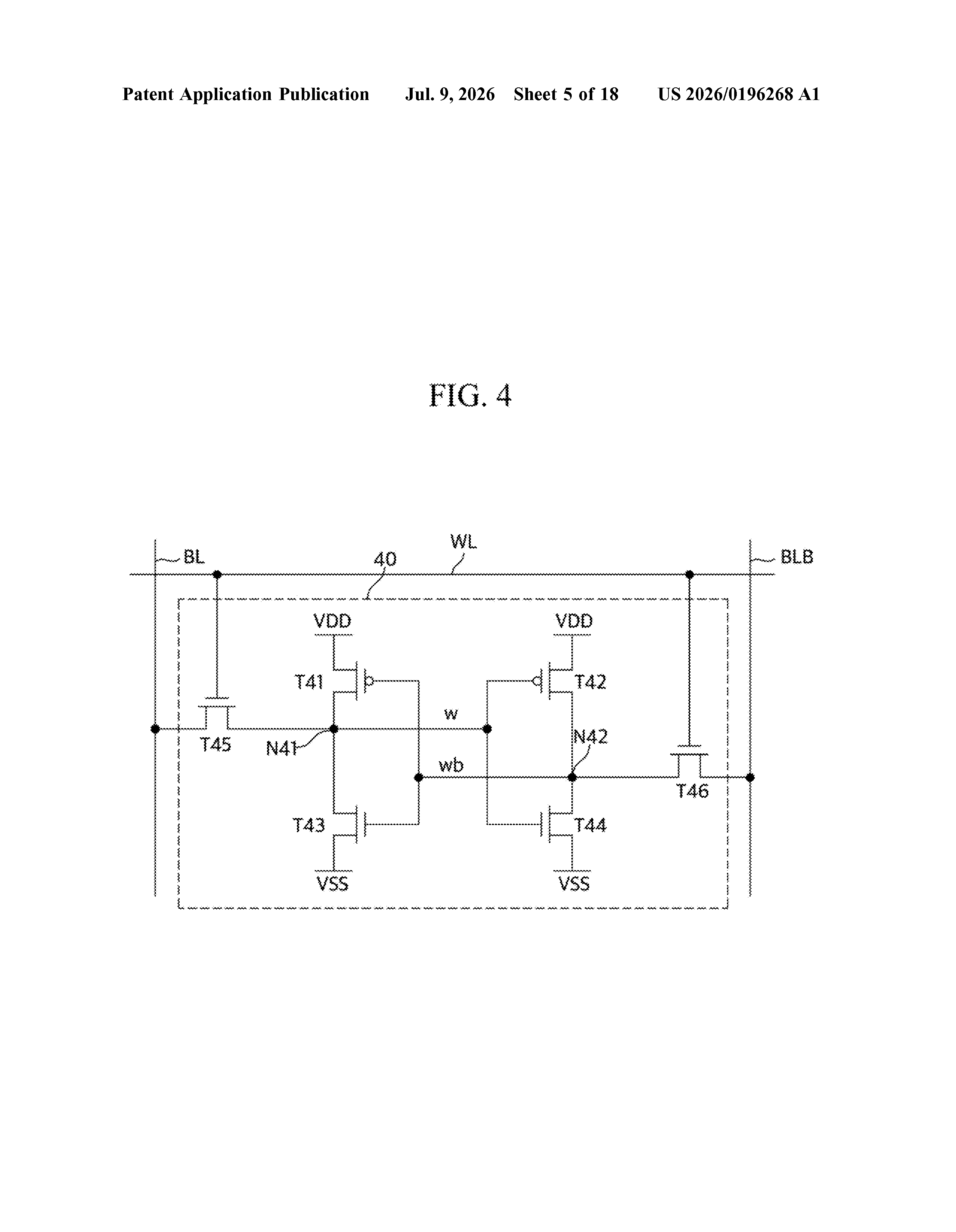
The patent describes a computing bit cell, a memory cell modified to also function as a logic element. A conventional memory cell just stores a single bit (a 0 or a 1). This cell stores a coefficient bit (a pre-loaded weight, like one parameter in a neural network) and then uses that stored value to influence a live calculation.
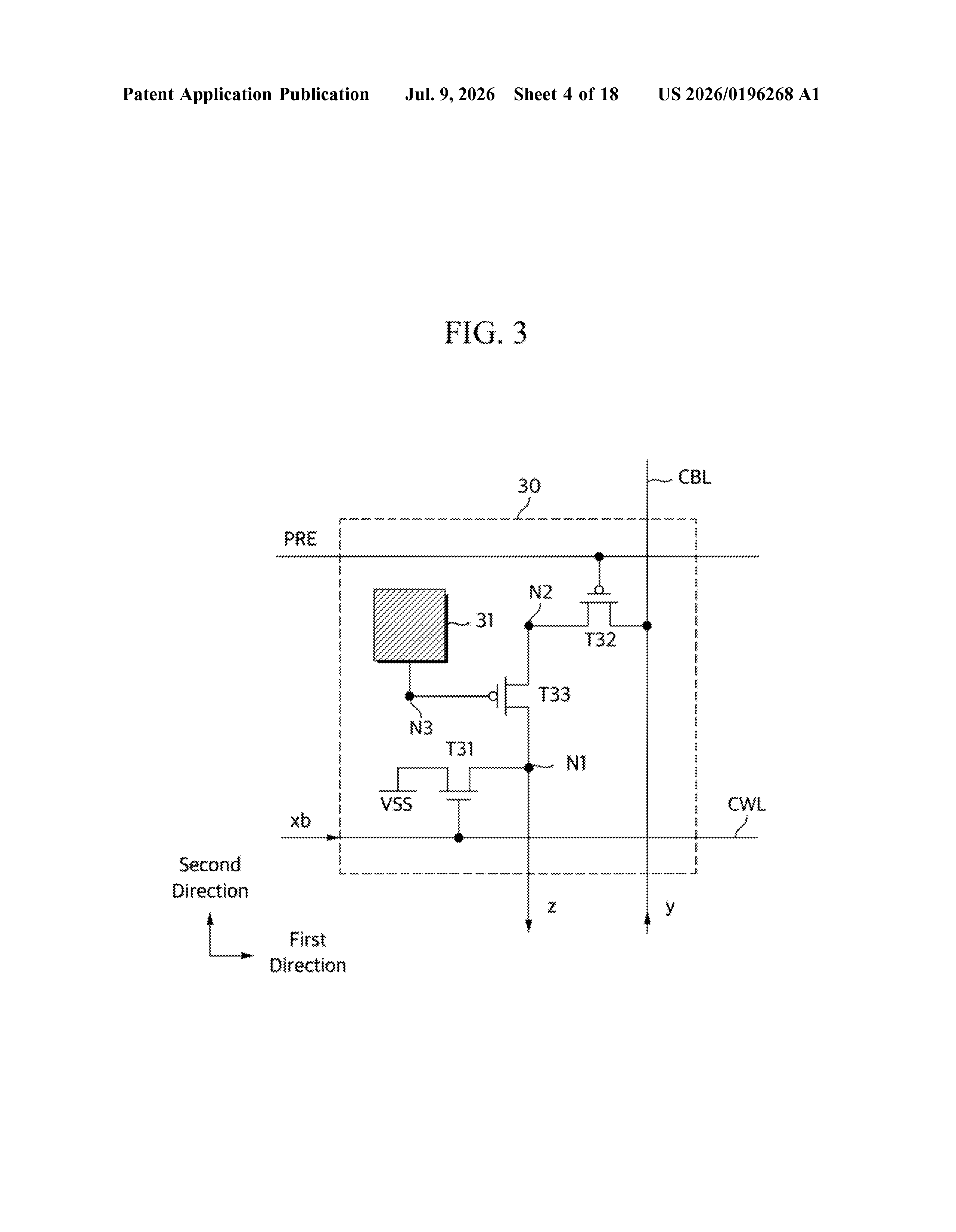
The cell contains three transistors working together:
- First transistor: connects to a horizontal wire that carries a voltage representing the first input bit. It controls whether current can flow to ground.
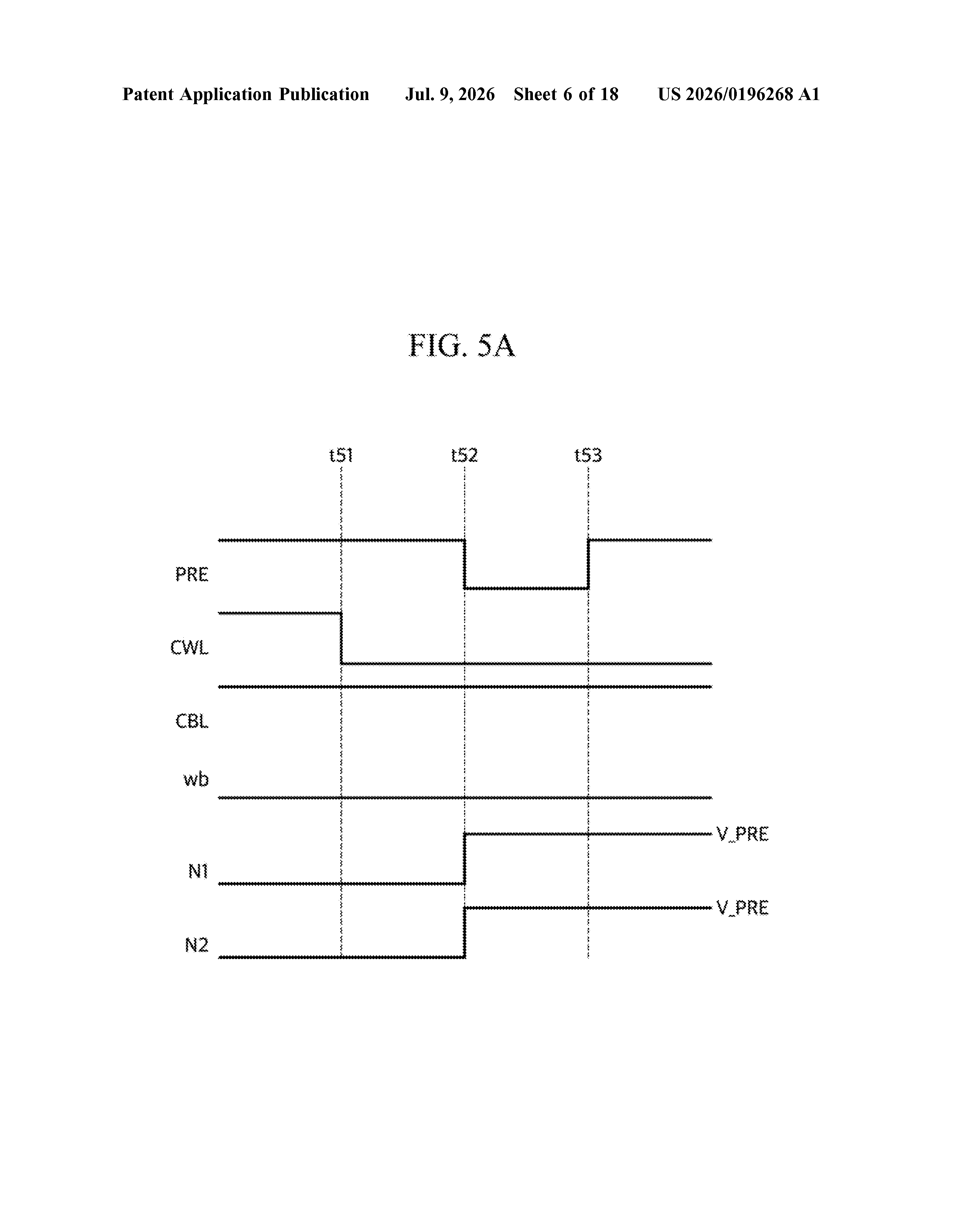
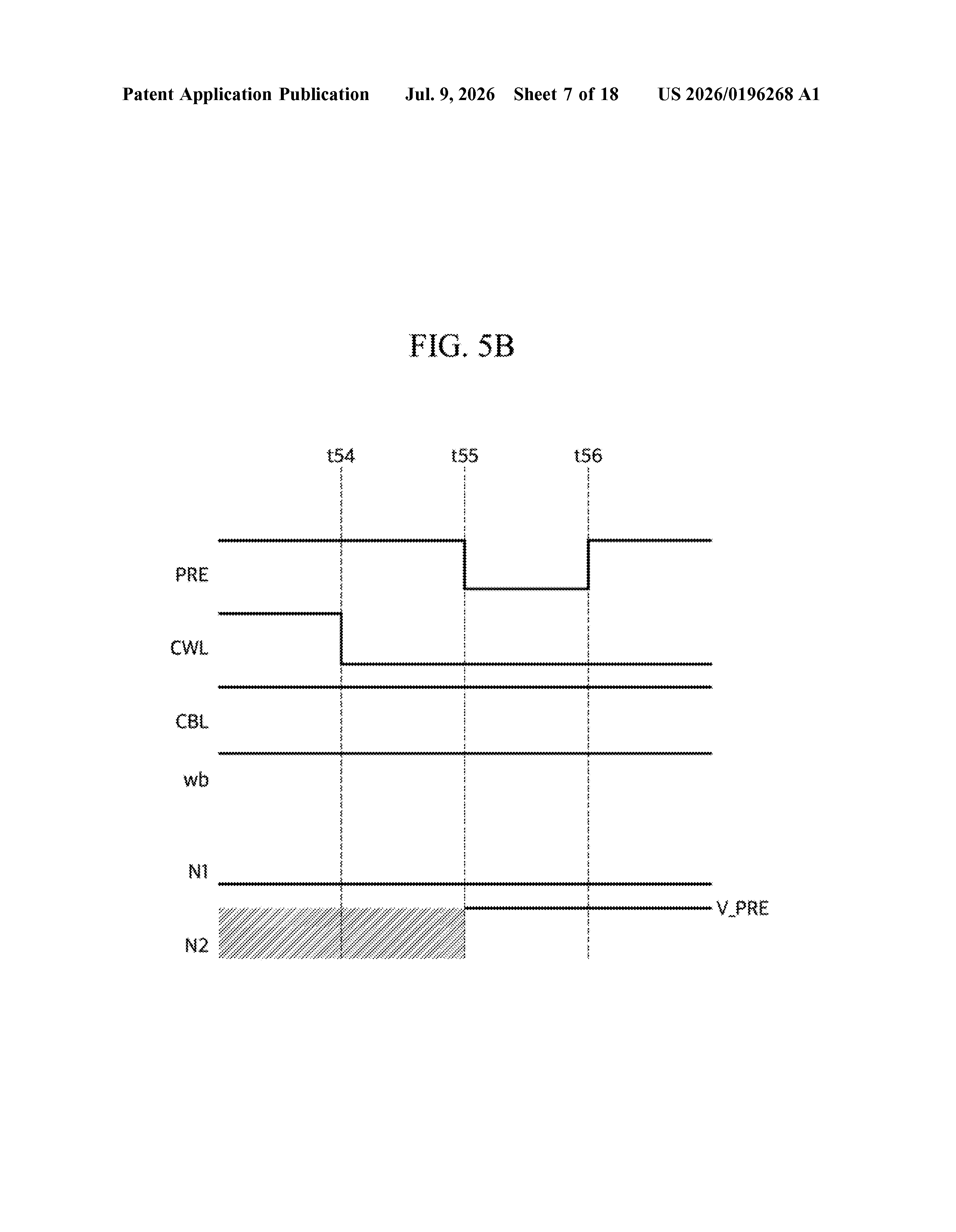
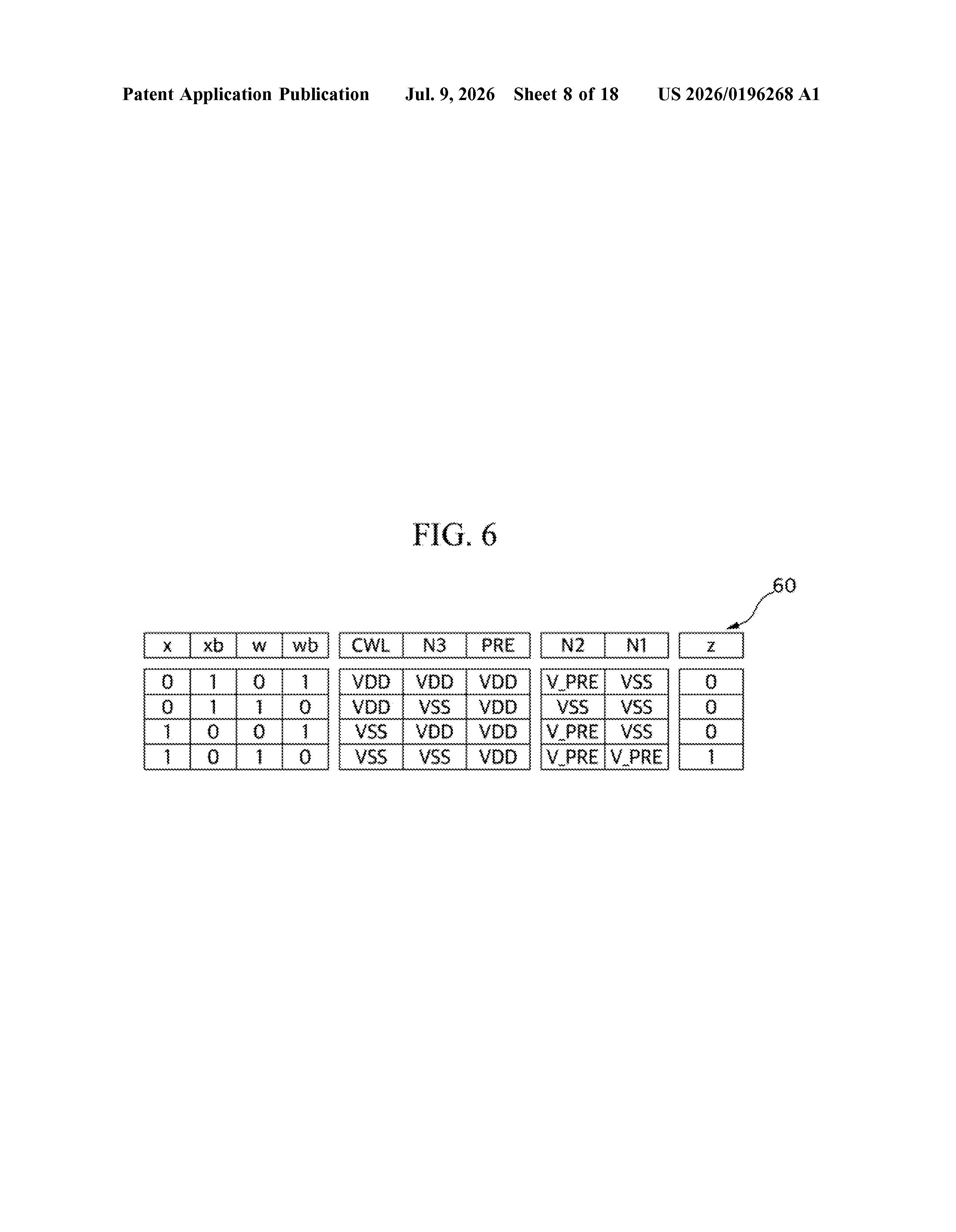
- Second transistor: connects to a vertical wire carrying the second input bit and is switched on or off by a pre-charge enable signal (a timing pulse that primes the circuit before a calculation).
- Third transistor: sits between the other two and is gated directly by the stored coefficient bit in the memory cell, so the stored value physically controls whether the two input signals interact.
The net effect is a bitwise multiply-accumulate operation (the core arithmetic of neural-network inference) performed inside the memory array itself. A control circuit manages the timing signals that sequence these operations across many cells in parallel.
What this means for AI chip power and speed
The phrase for this approach is compute-in-memory or processing-in-memory, and it's one of the more active areas in AI chip research right now. Moving data between memory and a central processor is one of the biggest sources of power consumption and delay in modern AI accelerators. Doing the multiplication inside the memory array attacks that problem at the source.
For you as a consumer, the downstream effect could be AI features that run faster on a phone or wearable without draining the battery as fast. For Samsung specifically, which makes both memory chips and system-on-chip processors, a patent in this space signals a real architectural direction, not just a research exercise.
This is a real engineering bet, not a trivial filing. Compute-in-memory architectures are genuinely hard to build at scale, and Samsung patenting a specific three-transistor cell design suggests the team has worked through enough of the implementation to commit it to paper. It's not flashy from the outside, but it sits close to the center of where AI chip design is heading.
Get our take in your Top Stories
Liked this breakdown? Add Patentlyze as a preferred source on Google, and our plain-English take shows up more often in your Top Stories the next time Samsung patent news breaks.
There are more where this came from
We read every patent application Big Tech publishes and send you the ones worth knowing. Plain English, free, every week.
The drawings
18 drawing sheets from US 2026/0196268 A1 · click any drawing to enlarge
Want this weekly breakdown for a company we don't cover? Patentlyze Pro →