
Samsung Patents an Automated System for Spotting Defects in Product Images
Every time Samsung makes a chip or a display panel, someone (or something) has to check whether it came out perfect. This patent describes a way to automate that check by precisely aligning a photo of the real product against a flawless reference image, then flagging every pixel that doesn't match.
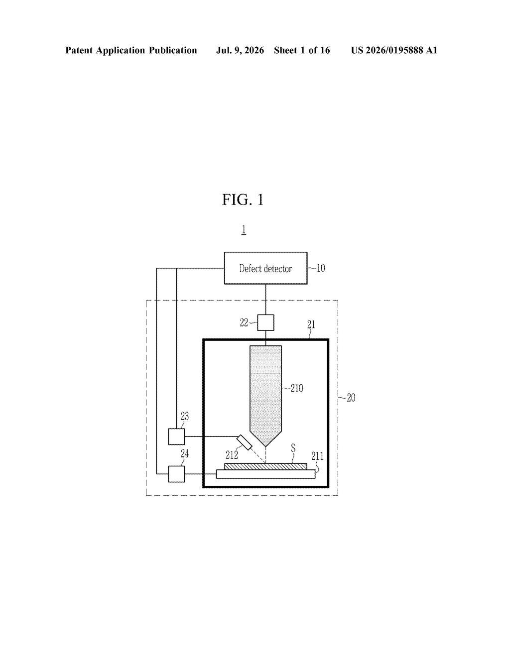
How Samsung's defect scanner compares photos to a perfect original
Imagine a quality inspector whose job is to compare a freshly printed circuit board against a master blueprint. They line up the two images as carefully as possible, then circle anything that looks wrong. That's exactly what this patent automates.
Samsung's approach chops the photo of a real product (the "target image") into smaller pieces, then slides each piece around the blueprint (the "reference image") until it finds the best possible match. By doing this in sections rather than all at once, the system can handle tiny misalignments much more reliably.
Once the two images are locked into position, the system subtracts one from the other. Any spot where the pixel values differ beyond a set threshold gets flagged as a defect. The result is an automated, repeatable inspection process that doesn't need a human eye.
How the segmented alignment and binarization threshold work
The patent describes a processor-implemented pipeline with four main stages:
- Segmentation: The target image (a photo of the item being inspected) is divided into multiple smaller sub-images.
- Similarity search: Each sub-image is slid across the reference image to find the region that looks most like it. This is essentially template matching, where the algorithm scores how closely two patches resemble each other.
- Index calculation in overlap regions: Where the target and reference overlap after each sub-image is matched, the system calculates an index value (a numeric score measuring alignment quality). The sub-image whose score is lower (meaning a tighter fit) wins, and its alignment offset is chosen as the final position.
- Defect detection via binarization: Once the images are aligned, the system computes the pixel-by-pixel difference between them. A binarization threshold (a cutoff value that converts a continuous difference into a simple yes/no: defect or not) is applied, and anything above the threshold is marked as a flaw.
The key insight is the two-pass segmentation strategy. Rather than trying to align the full image in one shot (which can fail if part of the product is slightly rotated or offset), it finds the best-matching segment first and uses that as the anchor for the final alignment.
What this means for Samsung's chip and display manufacturing
Samsung is the world's largest producer of memory chips and OLED display panels, and defect detection at that scale is a genuinely hard problem. Even a one-pixel misalignment between a target photo and a reference image can cause the system to flag a false defect or, worse, miss a real one. A segmented, multi-pass alignment approach directly addresses that problem and could mean fewer false rejects coming off the production line.
For consumers, better automated inspection typically translates to fewer defective screens and chips reaching finished products. For Samsung, it means lower waste and faster throughput. This patent sits squarely in the industrial machine-vision space, so the most likely home for it is inside Samsung's own fabrication facilities rather than in a consumer product.
This is a solid, focused manufacturing-automation patent with a clear practical application. It doesn't reinvent defect detection, but the segmented alignment strategy is a genuinely useful refinement for high-precision production lines where tiny misregistrations cause big quality problems. If you're not watching Samsung's fab-automation filings, this is a good reminder that the company invests heavily in the less glamorous side of making things.
Get our take in your Top Stories
Liked this breakdown? Add Patentlyze as a preferred source on Google, and our plain-English take shows up more often in your Top Stories the next time Samsung patent news breaks.
There are more where this came from
We read every patent application Big Tech publishes and send you the ones worth knowing. Plain English, free, every week.
Want this weekly breakdown for a company we don't cover? Patentlyze Pro →