
Samsung Patents a Storage Chip That Processes Data Without Sending It to the CPU
Most storage chips just hold data and wait to be asked for it. Samsung's new patent describes a chip that can also crunch that data itself, cutting out the round trip to the main processor entirely.
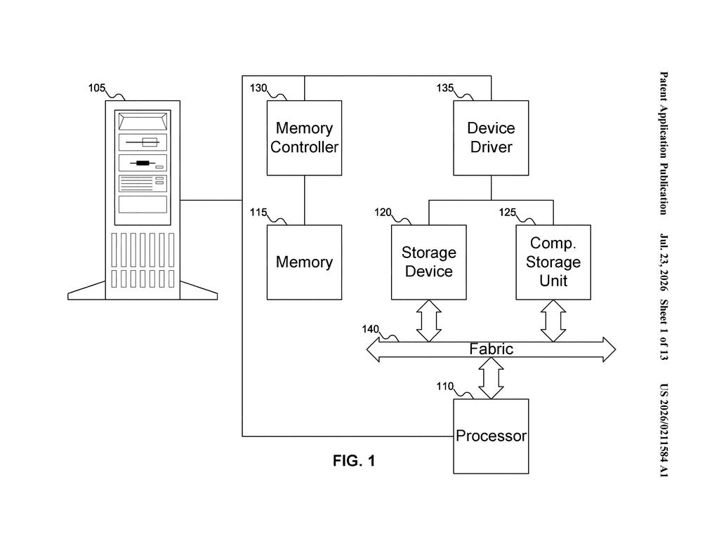
What Samsung's compute-inside-storage idea actually does
Imagine your filing cabinet could not only store your documents but also sort, summarize, and highlight them before handing them back to you. Right now, storage chips (like SSDs) just hold data. When your computer needs to do something with that data, it fetches it, sends it to the main processor (the CPU), waits for the CPU to do the work, and then gets the answer back. That back-and-forth takes time and uses energy.
Samsung's patent describes a computational storage unit that skips most of that journey. The storage chip itself runs the calculation on the data it's already holding, then hands back only the result. Your CPU sends one instruction and gets one answer, without ever moving the raw data out of storage.
This sounds like a minor plumbing fix, but moving data around is one of the biggest bottlenecks in modern computing, especially for AI and database workloads. Cutting that trip short can make systems noticeably faster and cheaper to run.
How a single command triggers storage, compute, and return
The patent describes a computational storage unit (CSU) made of three main parts working together:
- Storage: Where the raw data lives, just like a normal SSD or flash memory chip.
- Controller: The internal manager that reads data out of storage when needed.
- Computational engine: An on-chip processor that runs a specific function (think: filter, compress, search, or run an AI model layer) directly on that data.
The key detail is in how the system gets triggered. The host CPU sends a single command that bundles three things together: where the data is stored, which function to run on it, and where to put the result. The CSU handles everything from there internally and returns only the output.
This contrasts with today's standard approach, where the CPU has to issue separate commands to fetch data, load it into system memory, process it, and write results back. Each of those steps costs time and bus bandwidth (the capacity of the data highway connecting chips). By collapsing the sequence into one instruction, Samsung's design reduces the traffic on that highway significantly.
The patent is filed under storage and memory architecture classifications, suggesting this targets enterprise and data-center storage devices, not consumer laptops directly.
What this means for data-heavy workloads and AI hardware
The bottleneck in modern AI and database systems is often not the processor itself but the constant shuttling of data between storage and the CPU. A chip that processes data in place means less data on the move, which translates to lower power consumption and higher throughput for workloads like database queries, video transcoding, and AI inference.
For Samsung, which is both a major flash memory maker and a chip designer, this patent points toward higher-value storage products that compete on more than raw capacity or speed. It's a signal that Samsung sees the storage layer as a place to win on intelligence, not just gigabytes. Whether this appears in a specific product line soon is unclear from the filing alone, but the architecture is practical and the industry trend toward near-data processing is well established.
Computational storage is a real and growing area of hardware design, not a research curiosity. Samsung filing a patent here is a meaningful move because they have the manufacturing scale to actually ship this kind of chip. The single-command design described in the claim is clean and implementable, and it solves a real problem that bottlenecks AI and data-center hardware today.
There are more where this came from
We read every patent application Big Tech publishes and send you the ones worth knowing. Plain English, free, every week.
The drawings
13 drawing sheets from US 2026/0211584 A1 · click any drawing to enlarge


Want this weekly breakdown for a company we don't cover? Patentlyze Pro →
Be the first to weigh in