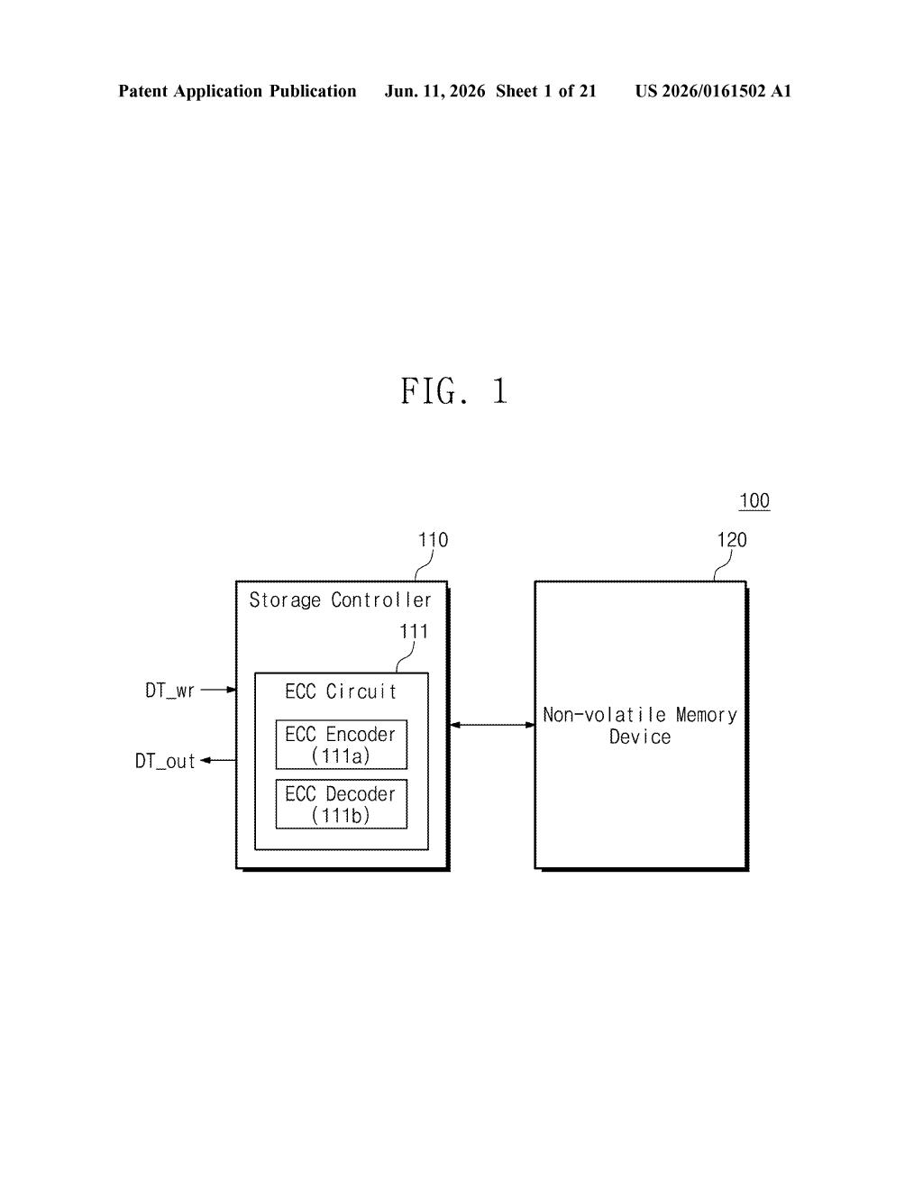
Samsung Patents a Two-Stage System to Catch and Fix Corrupted Data on Storage Drives
Every time your phone or SSD reads data, tiny errors can creep in — and catching them before they become real data loss is a surprisingly hard problem. Samsung's latest patent describes a smarter two-stage circuit designed to do exactly that, even when parts of the stored data are ambiguous.
What Samsung's two-stage storage error fix actually does
Imagine you're reading a blurry photocopy of a document. Some words are perfectly clear, but a section in the middle is smudged. A simple spell-checker might give up on the smudged part, but a better approach would be to first figure out what the clear parts say, use that context to make a best guess at the smudged section, and then run a full check on everything together.
That's essentially what Samsung's new error-correction circuit does for flash storage chips — the kind inside SSDs, smartphones, and data center drives. When your device reads data back from storage, some bits can be uncertain or corrupted. This circuit first handles those uncertain bits with an initial pass, makes an educated reconstruction of what they probably should be, and then sends the whole thing through a second, more powerful correction stage.
The end result is that the storage controller has a much better chance of recovering your data correctly, even as flash memory ages and becomes less reliable over time. It's the kind of behind-the-scenes engineering that keeps your files intact without you ever noticing.
How the virtual puncturing and reconstruction steps work
The patent describes an ECC (Error Correction Code) circuit — the hardware responsible for detecting and fixing bit errors in data read from flash memory. The key innovation is a two-decoder pipeline that handles a specific problem: portions of a stored codeword where the correct bit values are uncertain, which the patent calls a superposition region.
Here's how the pipeline works:
- Virtual puncturing: The first decoder temporarily sets the uncertain bits in the superposition region to a fixed placeholder value ("puncturing" — a standard ECC technique for handling unknown bits) and runs an initial decoding pass on the rest of the data to generate a first estimated codeword.
- Reconstruction: A dedicated reconstructed data generator uses both the original read data and that first estimate to make a smarter guess at what the superposition region's bits actually are, producing a second estimated codeword and then a full reconstructed codeword containing the data, main parity, and sub-parity bits.
- Main ECC decoding: Both decoders work together on the reconstructed codeword to perform a final, full error-correction pass and fix any remaining errors.
The approach is notable because it reuses the first decoder in both stages, which can reduce hardware complexity while still achieving better correction capability than a single-pass approach.
What this means for flash storage reliability at scale
Flash memory degrades with use — each write cycle makes individual memory cells slightly less reliable, which means the error rate of aging SSDs and NAND chips climbs over time. Better ECC hardware is one of the primary ways storage manufacturers extend the usable life of their chips and maintain data integrity in high-demand environments like data centers, where drives run flat-out around the clock.
For you as a consumer, this kind of work is invisible but important — it's the engineering that determines whether your SSD survives five years of heavy use or starts silently corrupting files at year three. For Samsung, which is one of the world's largest producers of NAND flash and SSDs, advances in on-chip ECC directly affect the competitiveness of everything from consumer drives to enterprise storage products.
This is solidly unglamorous but genuinely useful work. ECC circuit design is one of those fields where incremental improvements compound into real reliability gains at scale, and Samsung's two-stage reconstruction approach addresses a real limitation of simpler single-pass decoders. It won't make headlines outside storage engineering circles, but it's the kind of patent that quietly ends up in millions of devices.
Get one Big Tech patent every Sunday
Plain English, intelligent commentary, no hype. Free.
Editorial commentary on a publicly published patent application. Not legal advice.