Samsung Display Patents a Variable-Width Touch Sensor Electrode Layout
Most touchscreens use a perfectly uniform grid of electrodes — but Samsung's new patent deliberately makes those electrodes different sizes. The question is why, and whether it actually makes your screen smarter.
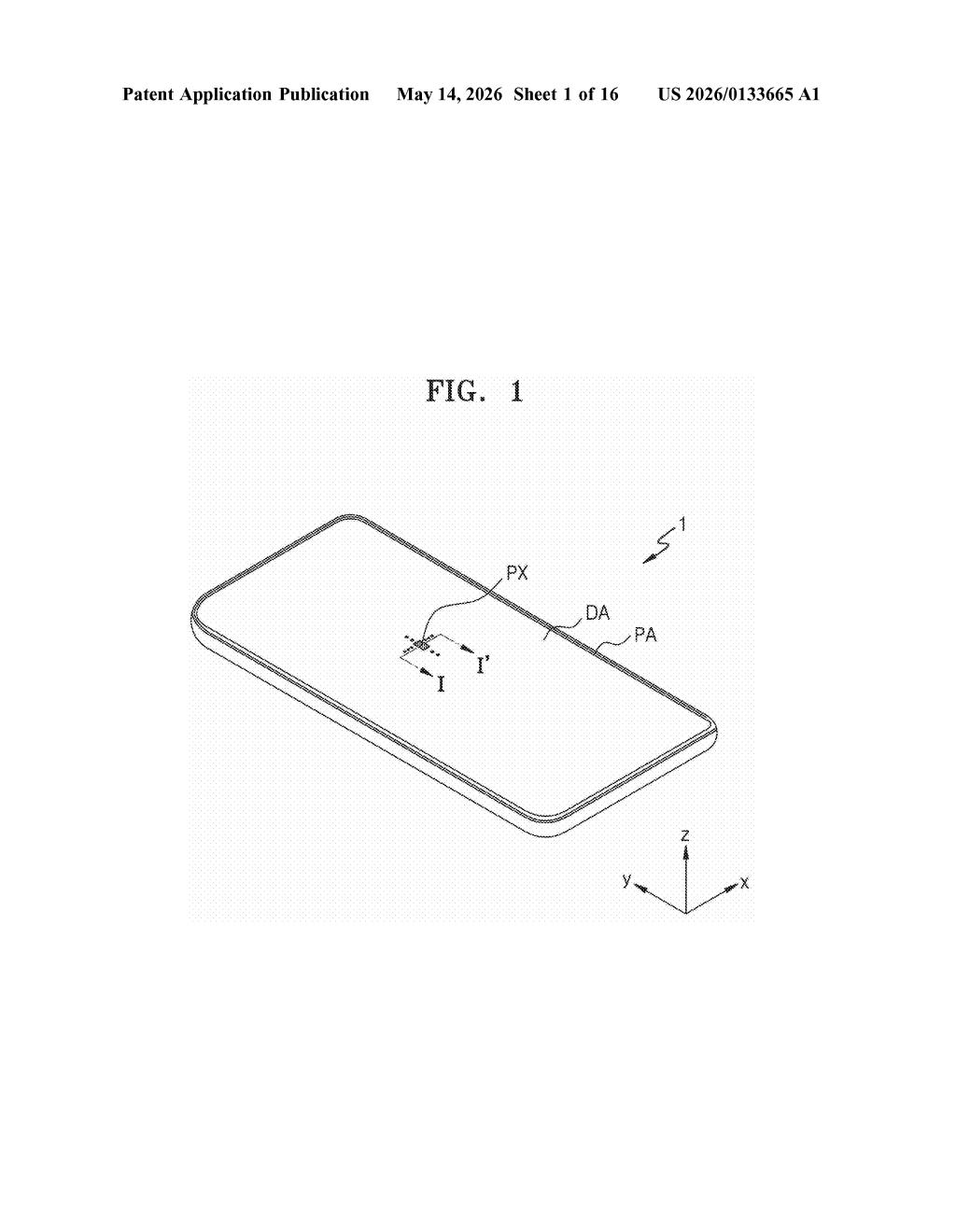
What Samsung's uneven touch electrode grid actually does
Imagine your phone's touchscreen as a city grid. Normally, every block is the same size, which makes routing easy but wastes space in awkward corners. Samsung's patent describes a touch sensor layout where some of those "blocks" — the electrodes that detect your finger — are deliberately different sizes depending on where they sit.
The screen has two types of sensor rows running in different directions. Where those rows share space, Samsung uses rectangular electrode sections of different areas to fill the gaps more efficiently. Think of it like fitting puzzle pieces rather than identical tiles.
The goal is likely better touch detection in the spaces between primary electrodes — those interstitial zones where your finger might land but signal strength traditionally drops off.
How the first and second electrode rows share sensing space
The patent describes a sensing area built from two sets of electrode rows oriented in perpendicular directions (a first direction and a second direction).
The key innovation is in the second sensor electrode row: instead of being a single uniform shape, it is divided into a first portion and a second portion, each rectangular, but with different areas. These portions sit in the gaps defined between the first sensor electrode rows — essentially occupying the interstitial space that a uniform design would either waste or fill symmetrically.
Why does the area difference matter? In capacitive touchscreens (the kind that read the tiny electrical field your finger disturbs), electrode size directly affects:
- Sensitivity — larger electrodes pick up weaker signals
- Spatial resolution — smaller electrodes localize touch more precisely
- Crosstalk — adjacent electrodes can interfere with each other
By varying the electrode areas in the fill zones, Samsung can tune those trade-offs locally — potentially boosting sensitivity where the first-row electrodes leave gaps, without sacrificing resolution everywhere else.
What this means for touch accuracy in future Samsung displays
For consumers, this kind of sub-electrode geometry work is invisible — but it's the type of patent that shows up later as improved touch responsiveness in spec sheets. If Samsung can extract better signal from the interstitial zones between primary rows, that could mean more reliable edge-of-screen gestures or stylus tracking in thinner display stacks.
The broader context is that as displays get thinner and OLED panels push electrode layers closer together, there's less room for brute-force uniform grids. Variable-area electrode layouts are one tool for squeezing more touch performance out of tighter physical constraints — relevant for foldables, rollables, and ultra-thin glass.
This is incremental display engineering, not a dramatic leap — Samsung Display files patents like this routinely as part of ongoing refinement of capacitive sensing layouts. It's worth noting as a signal that Samsung is actively optimizing electrode geometry for next-generation thin displays, but don't expect a product announcement based on this alone.
Get one Big Tech patent every Sunday
Plain English, intelligent commentary, no hype. Free.
Editorial commentary on a publicly published patent application. Not legal advice.