Samsung Display Patents a Gate Bypass Wiring System for Displays
Routing signals across a display panel sounds mundane — until the routing itself limits how thin or how precise a screen can be. Samsung Display's latest patent tackles exactly that problem with a new wiring trick called gate bypass auxiliary lines.
What Samsung's gate bypass auxiliary lines actually do
Imagine a city grid where traffic signals are controlled by a single road running along the edge of town. If that road gets congested or cut off, intersections across the whole city go dark. Modern display panels face a similar challenge: the circuits that tell each row of pixels when to light up need reliable signal paths, and the wiring layout can become a bottleneck.
Samsung Display's patent describes a display panel with an extra set of wires — called gate bypass auxiliary lines — that create a more direct electrical connection between the gate driving circuit (the part that sequences pixel rows) and the gate lines running across the screen. Instead of signals traveling through a single, potentially congested path, these bypass lines offer an alternative route.
The design also includes two sets of helper wires running in different directions across the panel, working alongside the main data lines. Together, they're meant to keep signal timing clean and consistent — which translates to sharper, more uniform images for you as a viewer.
How the bypass lines reroute gate signals in the panel
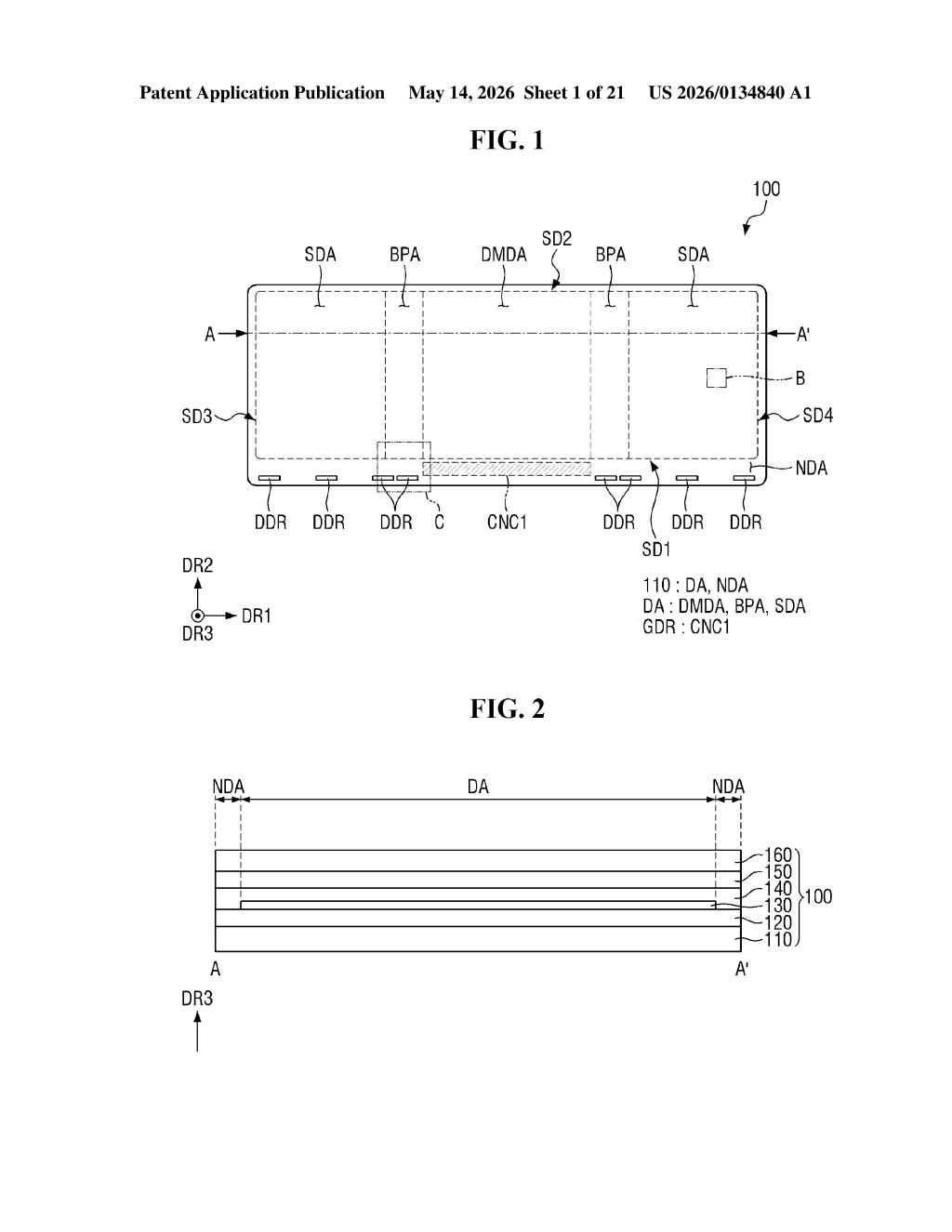
The patent describes a layered display structure built on a substrate divided into a display area (where pixels live) and a non-display area (the border region housing control circuitry). On top of the substrate sit a circuit layer — containing all the driving electronics — and an element layer where the actual light-emitting components reside.
Inside the circuit layer, the architecture gets specific:
- Gate lines run horizontally (first direction) and are stacked vertically (second direction) across the display area, telling pixel rows when to activate.
- Data lines run vertically, carrying the actual color and brightness information to each pixel.
- First auxiliary lines run horizontally alongside the gate lines.
- Second auxiliary lines run vertically, sitting adjacent to the data lines.
The key invention is that a subset of those second auxiliary lines are designated as gate bypass auxiliary lines. These wires create a direct electrical bridge between the gate lines and the individual stages of the gate driving circuit (the sequential logic blocks that activate one row at a time). Think of it like adding a dedicated express lane between the gate driver and each row of the panel, bypassing whatever congestion might exist on the primary path.
By embedding this bypass routing within the existing auxiliary line grid, Samsung avoids adding bulky new wiring layers — keeping the panel architecture compact.
What this means for thinner, cleaner display designs
Gate signal integrity is one of the less-glamorous but genuinely important factors in display quality. If gate timing drifts even slightly across a large panel — think a big OLED TV or a foldable phone screen — you can end up with visible line artifacts or brightness non-uniformity. Gate bypass auxiliary lines are a structural hedge against that, giving engineers more routing flexibility without ballooning the border width or adding new physical layers.
For Samsung Display, which supplies panels to its own Galaxy devices as well as other manufacturers, incremental wiring improvements like this compound over time into thinner bezels, higher yields, and better uniformity at scale. You probably won't see a spec sheet that says "now with gate bypass lines" — but it's the kind of foundational work that quietly enables the next generation of slimmer, more reliable screens.
This is deep-infrastructure display engineering — the kind of patent that matters a lot to panel process teams and almost no one else. It's not a flashy new display technology, but gate routing improvements genuinely affect manufacturing yield and image uniformity, so it's not trivial either. Worth noting as a signal that Samsung Display is actively optimizing its OLED panel architecture at the circuit-routing level.
Get one Big Tech patent every Sunday
Plain English, intelligent commentary, no hype. Free.
Editorial commentary on a publicly published patent application. Not legal advice.