Samsung Patents a Digital Twin System for Semiconductor Process Optimization
Building a chip is extraordinarily sensitive — tiny variations in temperature, pressure, or chemistry during fabrication can silently degrade a product that looks perfect on the surface. Samsung's new patent describes a digital twin approach that virtually mirrors real chip structures and stress-tests them in simulation before problems show up on the actual fab floor.
What Samsung's chip-simulation mirroring actually does
Imagine you're baking thousands of identical cakes, but the oven temperature drifts by a degree or two across batches. You'd want a way to predict which batches will fail before you taste them — not after. That's essentially the problem Samsung is solving here, but for semiconductor chips.
Samsung's method creates a virtual 3D copy (a "digital twin") of each chip structure at each step of the manufacturing process. It then runs stress tests inside that simulation and compares the results to real-world stress test data, tuning the simulation's variables until they match reality.
Once the simulation is calibrated against one type of stress test, Samsung can apply those learned variables to predict outcomes for a different stress test — one with at least one different process variable — without having to run every physical experiment from scratch. The goal is faster, cheaper, and more accurate yield optimization across chip generations.
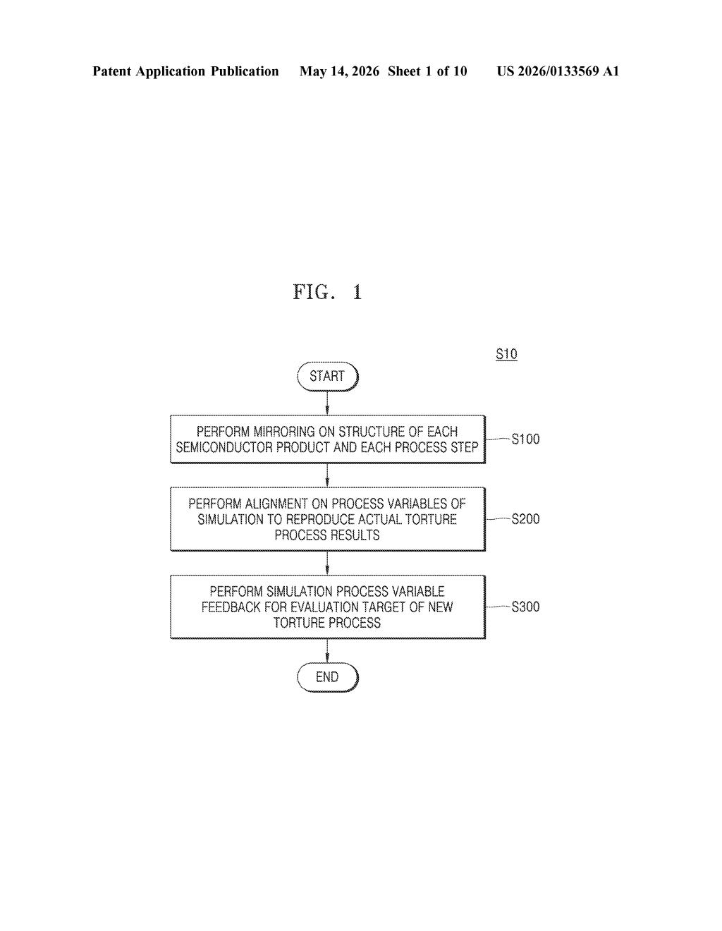
How the digital twin aligns and feeds back process variables
The patent describes a three-stage pipeline running on at least one processor:
- Mirroring: The system scans each semiconductor product structure at each process step and constructs a virtual 3D model that faithfully represents the physical structure. Think of it as a photorealistic digital replica of the chip at a given manufacturing stage.
- Process variable alignment: A simulation is run on the 3D model and its output is compared against data from a first stress test (a real-world physical reliability test). The system adjusts the simulation's process variables — things like temperature profiles, material thicknesses, or doping concentrations — until the simulation and the real test results agree. This is essentially automated calibration.
- Process variable feedback: Once calibrated, the system applies those learned variables to a second stress test scenario that differs from the first in at least one process variable. This lets engineers predict how a slightly different process configuration would behave under a new test regime, without running the full physical experiment again.
The method is split across a first device and a second device, suggesting a distributed or client-server architecture — possibly separating the computationally heavy 3D simulation from the data management or feedback logic.
What this means for semiconductor yield and fab efficiency
Semiconductor fabs operate on razor-thin yield margins where a 1% improvement in process consistency can translate to millions of dollars in recovered wafer output. A well-calibrated digital twin that can generalize across stress test types means Samsung could reduce the number of expensive physical reliability experiments needed during process development — speeding up the time from new process node to volume production.
For Samsung's foundry business, which competes directly with TSMC and Intel Foundry, this kind of simulation-driven optimization could be a meaningful differentiator. Customers care deeply about reliability data delivered quickly. If digital twin feedback can compress qualification cycles, that's a real competitive edge — even if it's entirely invisible to end users.
This is unsexy but genuinely important fab-floor infrastructure work. Digital twins for manufacturing have been a buzzword for years, but applying them rigorously to semiconductor process variable calibration — with explicit feedback loops between different stress test regimes — is a concrete and practical advance. Samsung is clearly investing in the simulation layer that sits behind its manufacturing process, and this patent is a reasonable signal of that strategy.
Get one Big Tech patent every Sunday
Plain English, intelligent commentary, no hype. Free.
Editorial commentary on a publicly published patent application. Not legal advice.