
Sony Patents an Image Sensor That Spots Sharp Edges Before the Photo Leaves the Chip
Most cameras figure out where the sharp edges in a scene are after the image data leaves the sensor. Sony is patenting a way to do it inside the sensor itself, at the hardware level, before any data goes anywhere.
What Sony's in-sensor edge detection actually does
Imagine your camera looking at a scene with a dark tree branch against a bright sky. The boundary between that dark branch and that bright background is called an edge, and knowing exactly where edges are is fundamental to almost everything cameras do, from autofocus to computational photography to machine vision.
Right now, figuring out where those edges sit is mostly a job for software or a separate processor chip. Sony's patent describes an image sensor that does this work inside the sensor itself, by comparing neighboring pixels directly in the circuitry that reads them out. Instead of shipping raw brightness values out and letting something else sort through them, the sensor can flag "yes, there's a sharp edge here" on the spot.
The practical payoff is a cleaner, faster signal with less electronic noise corrupting the edge call. When two nearby pixels are compared through a dedicated amplifier circuit designed specifically for that job, the result is more reliable than doing the same math downstream in noisier conditions.
How the differential circuit finds edges pixel by pixel
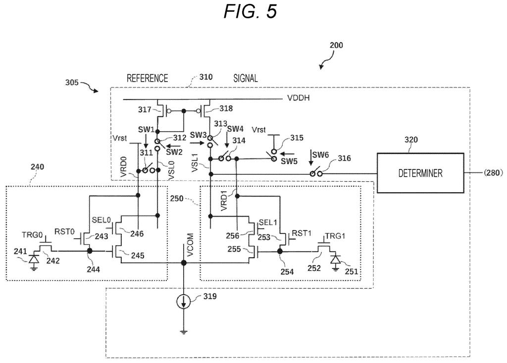
Sony's design organizes the pixel array into two groups: first pixels wired to one signal line and second pixels wired to a separate signal line. Each pixel contains a photoelectric conversion element (the light-absorbing part) and an amplification transistor that boosts the tiny electrical charge produced by incoming light into a readable voltage.
The key addition is a differential amplification circuit. A differential amplifier takes two input signals and outputs only their difference, which is a classic trick for canceling out noise that affects both inputs equally. Here, the two inputs are the amplification transistors of one selected first pixel and one selected second pixel sitting next to each other in the array.
A component called the determiner then reads the amplified difference and decides whether that voltage gap is large enough to indicate a real edge between those two pixels, meaning one pixel saw significantly more light than the other, or whether the gap is small enough to be the same region of the scene.
- Comparing pixels through a shared differential amplifier cancels common-mode noise (interference that hits both pixels equally)
- The edge decision happens at read-out time, inside the sensor
- No downstream processor needs to run a separate edge-detection pass on raw pixel data
What this means for cameras and computer vision devices
Image sensors are already doing more computation on-chip in every generation, from high-dynamic-range merging to phase-detection autofocus. Moving edge detection into the sensor fabric fits that same direction. For computer vision applications like robotics, automotive cameras, and security systems, knowing edge locations early and cleanly reduces the processing load on the main chip and can cut response latency.
For consumer cameras, the benefit is subtler but real: cleaner edge information means better autofocus, sharper demosaicing (the process that turns raw sensor data into a color image), and more accurate scene segmentation. The noise-suppression angle is the concrete engineering win here, since the differential approach is specifically designed to reject the kind of interference that plagues traditional single-ended pixel read-out.
This is a focused, technically solid patent on a specific read-out architecture improvement, not a headline product announcement. Sony Semiconductor Solutions supplies image sensors to a huge range of device makers, so incremental gains in on-chip processing quality matter at scale. The noise-suppression argument is real and well-established in analog circuit design. Worth tracking as a signal of where Sony's sensor roadmap is heading.
There are more where this came from
We read every patent application Big Tech publishes and send you the ones worth knowing. Plain English, free, every week.
The drawings
35 drawing sheets from US 2026/0222712 A1 · click any drawing to enlarge


Want this weekly breakdown for a company we don't cover? Patentlyze Pro →