Samsung Patents a Stacked 2D-Material Transistor with Vertical Channel Bridges
Samsung is patenting a transistor design that stacks multiple 2D semiconductor channels — like sheets of atomically thin material — both horizontally and vertically inside a single device. It's an architectural bet on what comes after silicon starts running out of room.
What Samsung's layered 2D transistor actually does
Imagine trying to pack more lanes onto a highway, but you've already used up all the horizontal space. The solution? Build upward — and then connect those upper and lower lanes with vertical ramps so traffic flows smoothly between them. That's essentially what Samsung is doing here, but with electrons instead of cars.
Conventional transistors control current through a single channel of semiconductor material. Newer designs stack multiple horizontal channels on top of each other (think of nanosheet transistors). Samsung's twist is adding a vertical channel that physically bridges adjacent horizontal layers, forming a connected 3D lattice inside one transistor.
Critically, every channel — horizontal and vertical — is made from a two-dimensional (2D) semiconductor material. These are ultra-thin materials (like MoS₂ or similar compounds) that are just a few atoms thick. That thinness is the whole point: it lets engineers pack more channel area into a tiny space without the quantum-mechanical leakage problems that plague traditional silicon at small scales.
How the horizontal and vertical channels connect inside the FET
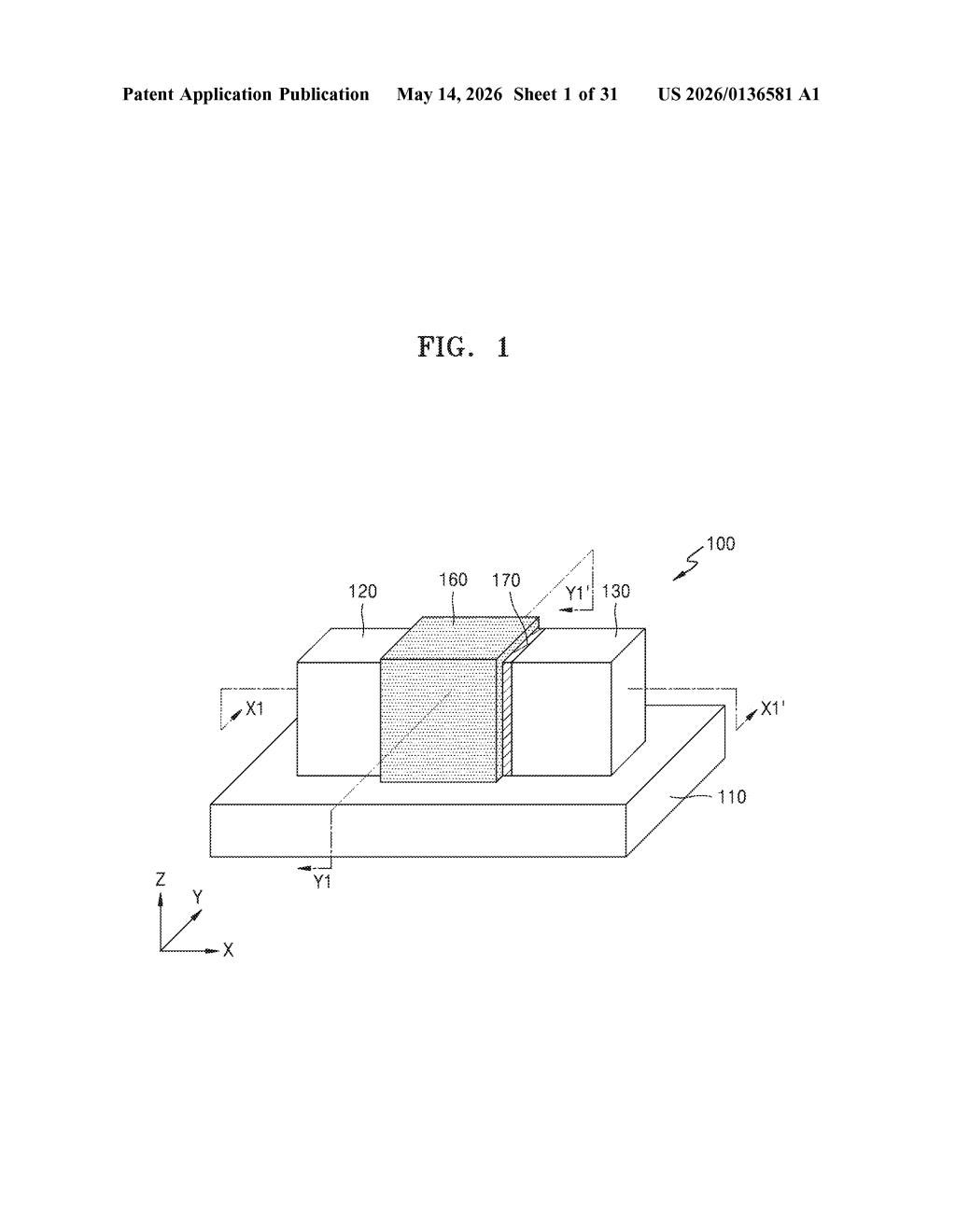
The transistor described in this patent has a source electrode and a drain electrode sitting on a substrate, separated along a horizontal axis. Between them, multiple horizontal channels are stacked vertically above the substrate — each one a sheet of 2D semiconductor material.
The novel element is the vertical channel: a connector made of the same 2D material that fills the gap between two adjacent horizontal layers and also runs the full length from source to drain. So instead of isolated stacked sheets, you get an interconnected mesh.
- First gate electrode: A control electrode that faces all the channels — both horizontal and vertical — so a single gate signal modulates current across the entire structure.
- Gate insulating layer: Electrically isolates the gate from the channels and electrodes, preventing leakage while allowing electrostatic control.
- 2D semiconductor material: Each channel independently uses an atomically thin semiconductor — likely a transition metal dichalcogenide (TMD) such as MoS₂ or WSe₂ — which offers strong electrostatic controllability and reduced short-channel effects (unwanted current leakage that worsens as transistors shrink).
The architecture effectively multiplies usable channel area without expanding the transistor's footprint, which is the core scaling challenge for sub-2nm chip design.
What this means for transistor scaling beyond silicon
As silicon transistors approach their physical limits, chipmakers need materials and geometries that can keep delivering performance gains. 2D semiconductors have been a research darling for years precisely because their atomic thinness gives engineers fine-grained control over electrons — but manufacturing them at scale has been the hard problem. A patent like this signals Samsung is seriously mapping out device architectures, not just material research.
For you as a tech watcher, the practical implication is that future Samsung chips — in smartphones, AI accelerators, or memory controllers — could squeeze meaningfully more switching capacity into the same die area. The vertical channel bridging concept is an architectural efficiency play: more current path, same gate footprint.
This is deep semiconductor research territory — not a product announcement and not a near-term feature. But Samsung filing architecture patents that combine stacked nanosheet geometry with 2D materials is a meaningful data point: they're not just following TSMC and Intel on silicon nanosheets, they're exploring a divergent path. Worth bookmarking if you follow the post-silicon roadmap.
Get one Big Tech patent every Sunday
Plain English, intelligent commentary, no hype. Free.
Editorial commentary on a publicly published patent application. Not legal advice.