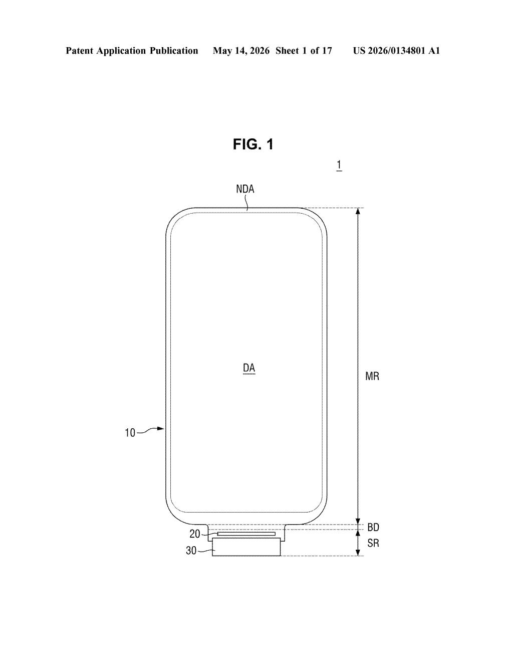
Samsung Display Patents a Diagonal Wire Routing Trick for Denser Pixel Layouts
Fitting more pixels into a smaller space without crossing wires is one of the unglamorous but very real engineering puzzles in display design. Samsung Display's latest patent tackles it with a carefully angled connecting wire that threads between existing pixel structures.
What Samsung's oblique connecting wire actually does
Imagine a city grid where every block is packed with buildings and you need to run a new water pipe from one street to another — but you can't dig up any existing infrastructure. You'd need to angle your pipe diagonally through the gaps. Samsung Display is doing something similar inside a display panel.
Each pixel in a screen needs its own data line — a tiny wire that tells it how bright to glow. The problem is that as screens get denser, routing those wires without them bumping into each other (or the pixel transistors sitting underneath) gets tricky. This patent describes a connecting wire with two sections: one that runs straight, and one that goes diagonal — specifically angled to hop over an adjacent pixel's structures without creating a short circuit.
It's not flashy, but this kind of precision wiring geometry is exactly what separates a manufacturable high-density display from one that's theoretically possible but practically impossible to build.
How the angled wire sections route around existing pixel structures
The patent covers a wiring architecture for a display panel where two neighboring pixels share a routing challenge: the second pixel's data line needs to connect to a signal wire, but to get there it has to pass over the first pixel's territory.
The solution is a connecting wire split into two sections:
- First section — runs straight (in the first direction) and is positioned so it overlaps the gate electrode of the transistor in the adjacent first pixel. Because it's on a different conductive layer, it can cross without making electrical contact.
- Second section — runs at an angle (oblique relative to both data lines) and overlaps the first pixel's data line. The diagonal path lets it navigate around the geometric constraints imposed by the pixel grid.
The key engineering insight is that by going diagonal in the second section, the wire can bridge between two parallel signal lines without requiring additional routing space in the horizontal or vertical axes. This matters most in high pixel-per-inch (PPI) panels — like those used in OLED displays for phones or VR headsets — where every micron of layout space is contested.
The claim specifically calls out that the second section overlaps the first signal line while the first section overlaps a transistor gate electrode — meaning the geometry is carefully constrained so the crossing points are predictable and electrically safe.
What this means for high-density OLED and display panels
For display engineers, wire routing at high pixel densities is a genuine bottleneck. As Samsung and others push toward higher-resolution OLED panels — for smartphones, foldables, and AR/VR headsets — the metal interconnect layers inside the panel become increasingly crowded. A patented diagonal routing scheme gives Samsung Display a documented, defensible approach to solving a layout conflict that would otherwise require a more complex (and potentially thicker) layer stack.
For end users, the downstream effect could show up as higher display resolution in future devices, or thinner panels that don't sacrifice brightness or refresh rate. It's not the kind of feature you'd ever see in a spec sheet, but it's the kind of foundational work that makes everything else possible.
This is a textbook display-interconnect patent — narrow, specific, and squarely in the 'infrastructure' category of IP. It won't make headlines, but Samsung Display files these kinds of layout geometry patents to protect manufacturing know-how that competitors would otherwise copy freely. It's worth a glance if you follow display fabrication, but it's not a window into any dramatic new product direction.
Get one Big Tech patent every Sunday
Plain English, intelligent commentary, no hype. Free.
Editorial commentary on a publicly published patent application. Not legal advice.