Samsung Patents a Gate-Bridging Architecture for Next-Gen Nanosheet Transistors
Samsung is patenting a clever structural trick that electrically ties together gate electrodes sitting on opposite sides of an isolation wall — a move that could help shrink transistor designs without sacrificing control over individual channels.
What Samsung's gate connection layer actually does
Imagine a tiny light switch inside a chip. Modern chips have billions of these switches — called transistors — and making them work reliably at smaller and smaller sizes is the central challenge of semiconductor engineering. This patent is about a very specific part of that switch: the gate electrode, which controls whether current flows through the transistor.
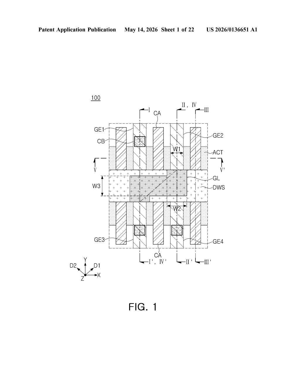
Samsung's design uses what it calls a gate connection layer — essentially a conductive bridge that sits on top of an insulating wall (the isolation structure) and links two separate gate electrodes together. This matters because at advanced chip scales, you sometimes need gates in different physical locations to act in unison, and routing that connection cleanly without creating interference is tricky.
The underlying transistor here is a nanosheet (or gate-all-around) type, which wraps the gate around thin layers of silicon channel material from all sides. That's the architecture Samsung and others are using to push beyond the limits of older FinFET designs.
How the gate connection layer bridges isolated electrodes
The patent describes a gate-all-around (GAA) nanosheet transistor — a transistor where multiple thin silicon sheets (channel layers) are stacked vertically and the gate electrode wraps completely around each one. This gives the gate more control over current flow compared to older fin-shaped transistors.
The key innovation is a gate connection layer that electrically bridges a first gate electrode and a second gate electrode. These two gates are physically separated by an isolation structure — an insulating wall that keeps different transistor cells from interfering with each other. The connection layer sits directly on top of that isolation structure and contacts its upper surface, forming a routed conductive path without penetrating into the active device region below.
The geometry is precisely specified using four directions:
- First direction: the base structure runs along this axis
- Second direction: gate electrodes extend this way (perpendicular to the first)
- Third direction: channel layers stack in this vertical axis
- Fourth direction: the diagonal or oblique direction separating the two gates being connected
By specifying that the gate connection layer sits on the upper surface of the isolation structure, Samsung is defining a fabrication-friendly routing scheme that avoids adding new insulating layers just to run the interconnect.
What this means for Samsung's advanced logic chips
For Samsung, this is foundational IP for its GAA transistor process nodes — the manufacturing technology it calls Multi-Bridge Channel FET (MBCFET), already in production at 3nm and planned for future nodes. The ability to connect gates across an isolation structure cleanly is exactly the kind of detailed structural claim that matters when licensing or defending a manufacturing process.
For you as someone watching the chip industry, this patent represents the unglamorous but essential work of locking down structural details before competitors can claim similar approaches. It won't make headlines the way a new chip announcement does, but these foundational device-architecture patents are the legal scaffolding that advanced process nodes are built on.
This is highly specialized semiconductor device IP — the kind of tightly scoped structural patent that matters enormously in chip manufacturing litigation and licensing but won't move markets on its own. Samsung is clearly building a dense portfolio around GAA/nanosheet transistor architecture, and this gate-bridging claim is a useful piece of that puzzle. Worth noting for anyone tracking Samsung Foundry's IP strategy, but not a product story.
Get one Big Tech patent every Sunday
Plain English, intelligent commentary, no hype. Free.
Editorial commentary on a publicly published patent application. Not legal advice.