Samsung Patents a Structural Defense Against Crack Spread in Semiconductor Chips
Cracks in semiconductor chips aren't just cosmetic — they can silently kill a device long after it leaves the factory. Samsung's latest patent describes a built-in physical barrier system designed to stop those cracks before they spread.
How Samsung's chip design physically stops cracks cold
Imagine a chip like a stack of extremely thin, fragile glass pancakes. When that stack gets cut, dropped, or stressed during manufacturing, tiny cracks can form at the edges — and those cracks have a nasty habit of traveling inward, eventually reaching the parts of the chip that actually do the computing.
Samsung's patent describes a way to physically trap those cracks before they go anywhere dangerous. The design adds special structural features — a crack-stopping wall and a recessed trench — built right into the chip's insulating layers near the outer edge. Think of it like a firebreak in a forest: you carve out a gap so the fire (or crack) has nowhere to go.
This isn't software or firmware — it's pure chip architecture. The goal is to make chips more physically resilient, which matters most during the dicing (cutting) process when wafers are sliced into individual chips, and during the stresses of packaging and real-world use.
How the blocking trench and prevention structure intercept cracks
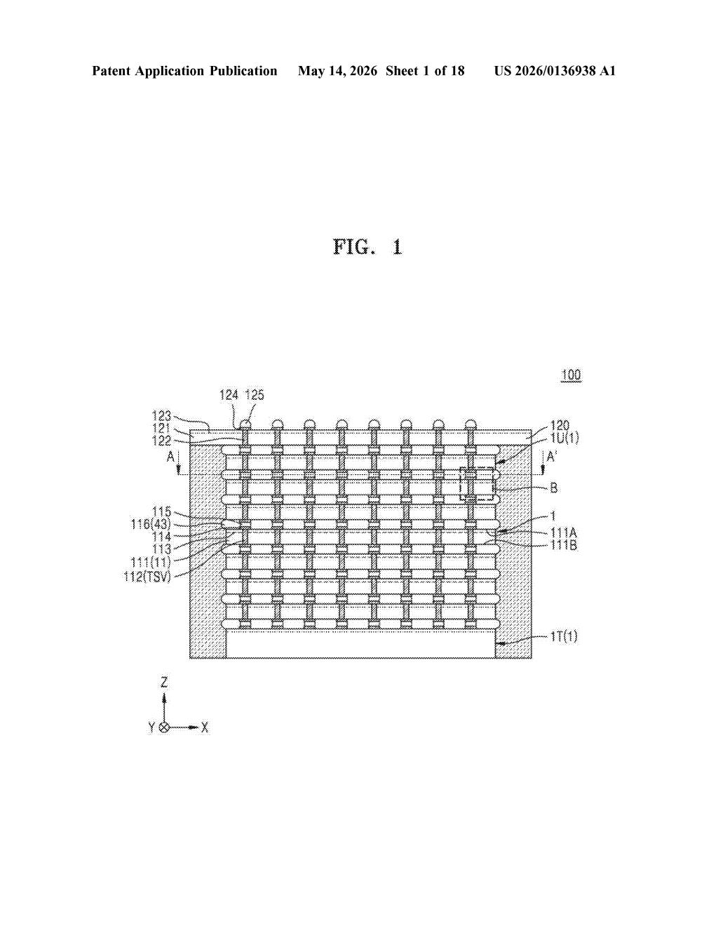
The patent describes a multilayer semiconductor chip structure with two key crack-control features working in tandem.
First, there's the crack propagation prevention structure — a physical barrier embedded in the chip's insulating stack, positioned between the inner circuitry region and the outer edge region. This structure sits on the device interlayer insulating layer (the insulating material sandwiched between the active transistor layer and the wiring layers above it) and is flanked on both sides by insulating layer side surfaces that face inward toward the logic and outward toward the chip edge.
Second — and this is the clever bit — there's a first blocking trench cut between that prevention structure and the inner insulating layer side surface. This trench is recessed downward from the top surface of the chip's upper insulating stack, pointing toward the substrate below. The trench acts as a stress-relief gap: if a crack gets past the outer barrier, the trench interrupts the mechanical continuity of the material, giving the crack nowhere to continue propagating.
- Substrate: the silicon base
- Device layer: where transistors live
- Wiring layer: metal interconnects routing signals
- Upper insulating stack: protective dielectric layers on top
The two-barrier approach — wall plus trench — gives the design redundancy: even if one mechanism fails, the other can stop crack advance.
What this means for chip yield and packaging durability
Chip yield (the percentage of usable chips cut from a wafer) is one of the most expensive variables in semiconductor manufacturing. Edge cracking during dicing is a well-known culprit for yield loss, and it gets worse as chips are made thinner and stacked higher in advanced packaging like HBM or 3D-NAND. A passive structural fix baked into the chip design — rather than requiring a process change — is an attractive and cost-effective approach.
For Samsung specifically, this kind of reliability engineering matters across its broad product portfolio: from the NAND flash in your SSD to the application processors in Galaxy phones. If this structure can reduce crack-related failures in high-volume manufacturing even modestly, the yield and reliability gains compound quickly at Samsung's scale.
This is a solid, unglamorous piece of semiconductor engineering — the kind that quietly saves millions of dollars in yield losses but never makes a product keynote. It's not a flashy AI or memory architecture patent, but crack mitigation in advanced packaging is a real and growing problem as chips get thinner and stacked packaging becomes the norm. Worth a look if you follow semiconductor manufacturing or reliability engineering.
Get one Big Tech patent every Sunday
Plain English, intelligent commentary, no hype. Free.
Editorial commentary on a publicly published patent application. Not legal advice.