Samsung Patents a Strain-Gradient Memory Cell to Boost DRAM Performance
Samsung is trying to squeeze more performance out of DRAM by using physical stress — literally bending the crystal structure of a material — to generate an electric field that helps control memory cells.
What Samsung's strain-polarized memory cell actually does
Imagine a tiny spring coiled just a little too tight. That tension doesn't just sit there — it pushes on everything around it. Samsung's patent applies the same idea to memory chips: by engineering a material that's under varying degrees of physical stress, you can coax it into producing a useful electric field, without needing extra wiring or power to create that field.
In a DRAM memory cell, transistors need precise electric fields to switch on and off reliably. Traditionally, you'd use additional layers or voltages to supply that field. Samsung's approach instead uses a strain gradient — a gradual change in internal mechanical stress across a special material layer called the "electric field generating pattern" — to create a built-in electric polarization. A thin buffer layer sits between the main semiconductor pillar and this special material, and it's that interface that kick-starts the strain.
The upshot is that the memory cell can potentially be controlled more efficiently, which matters a lot when you're cramming billions of these cells onto a chip the size of a fingernail.
How the buffer layer creates Samsung's strain gradient
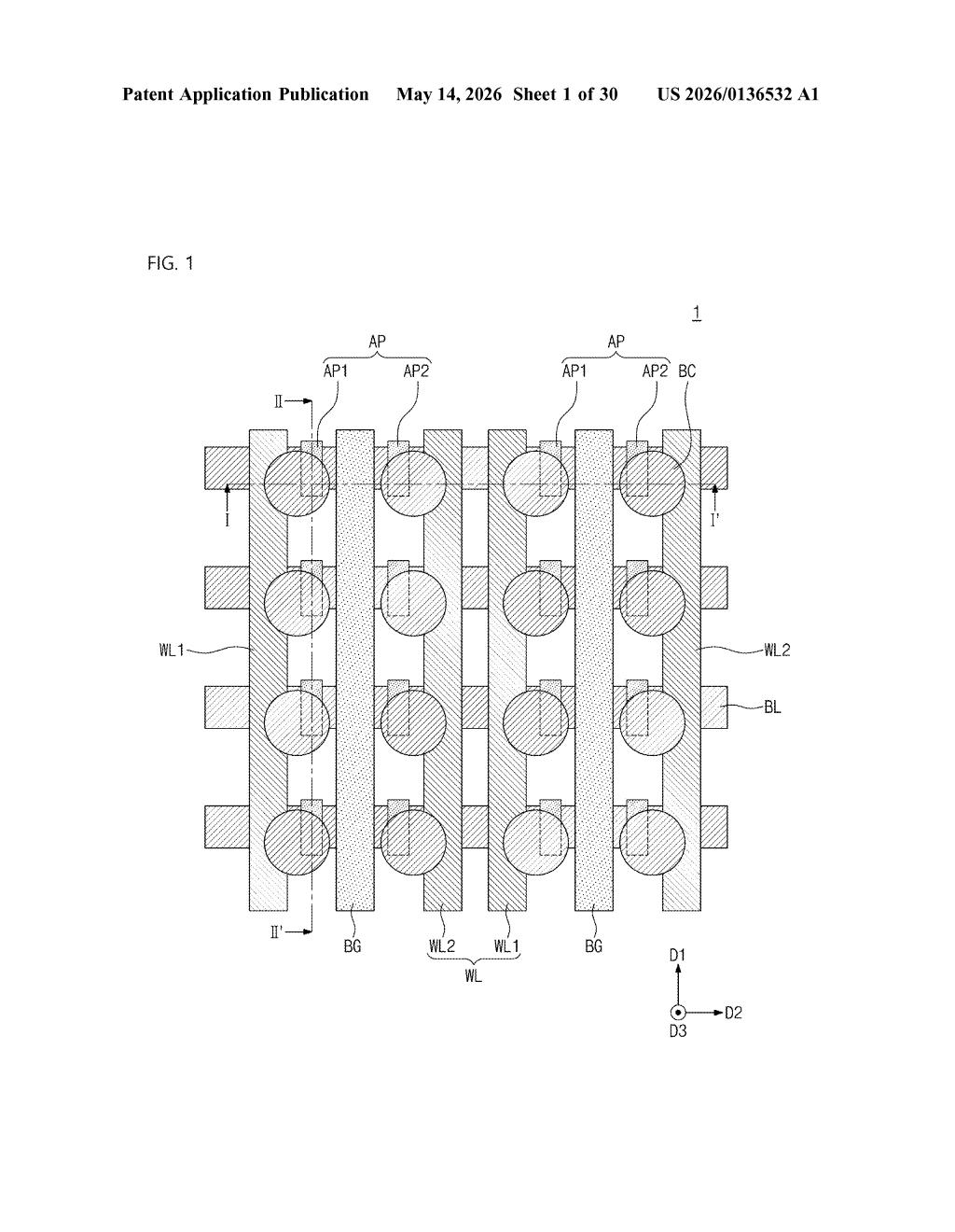
The patent describes a vertical DRAM-style memory cell — the kind used in modern high-density chips where transistors stand upright like skyscrapers rather than lying flat. The core structure includes:
- A bit line at the base (the wire that reads and writes data)
- A vertical active pattern — the semiconductor pillar that forms the transistor body
- A word line running horizontally to switch the transistor on or off
- A gate insulating pattern between the word line and the pillar (standard transistor insulation)
- An electric field generating pattern placed beside the pillar in both horizontal directions
- A buffer layer sandwiched between the pillar and that electric field material
The clever part is the strain gradient inside the electric field generating pattern. A strain gradient means the material is compressed or stretched by different amounts at different depths — tight near the buffer layer interface, relaxing further inside. This uneven stress triggers a phenomenon called flexoelectricity (electric polarization caused by mechanical strain variation, rather than uniform stress), producing a built-in electric field without any extra applied voltage.
The buffer layer isn't just structural filler — its lattice mismatch with the electric field generating material is likely what seeds that gradient in the first place, giving Samsung fine-grained control over the polarization strength.
What this means for next-gen DRAM density and speed
For DRAM scaling, every extra voltage source or structural layer you can eliminate is a win. As cell dimensions shrink below 10nm, fitting in the components needed to reliably switch a transistor gets brutally hard. A self-polarizing material that provides its own internal field — powered by strain rather than a dedicated circuit — could let Samsung pack cells tighter while maintaining the electric field strength needed for reliable reads and writes.
This also fits into a broader industry push toward ferroelectric and flexoelectric materials in memory. Competitors like Micron and SK Hynix are pursuing similar physics-bending tricks. Samsung staking out this specific vertical-cell architecture with a buffer-layer-seeded strain gradient is a way of carving out IP space in what's shaping up to be a key battleground for next-generation DRAM and storage-class memory.
This is deep-in-the-stack semiconductor physics work — not a product announcement, not AI software. But Samsung's memory division lives or dies on exactly these kinds of incremental structural innovations, and a built-in electric field that requires no extra power draw is genuinely useful at sub-10nm geometries. It's worth watching as a signal of where vertical DRAM cell design is heading.
Get one Big Tech patent every Sunday
Plain English, intelligent commentary, no hype. Free.
Editorial commentary on a publicly published patent application. Not legal advice.