Samsung Patents a New Contact Pad Layout for 3D Memory Wordlines
As 3D NAND flash stacks more and more memory layers on top of each other, the tiny metal contact pads that connect each layer's wordlines become a serious space problem. Samsung's latest patent proposes a specific alignment scheme to make that wiring geometry work more cleanly at extreme layer counts.
What Samsung's stacked memory wiring trick actually does
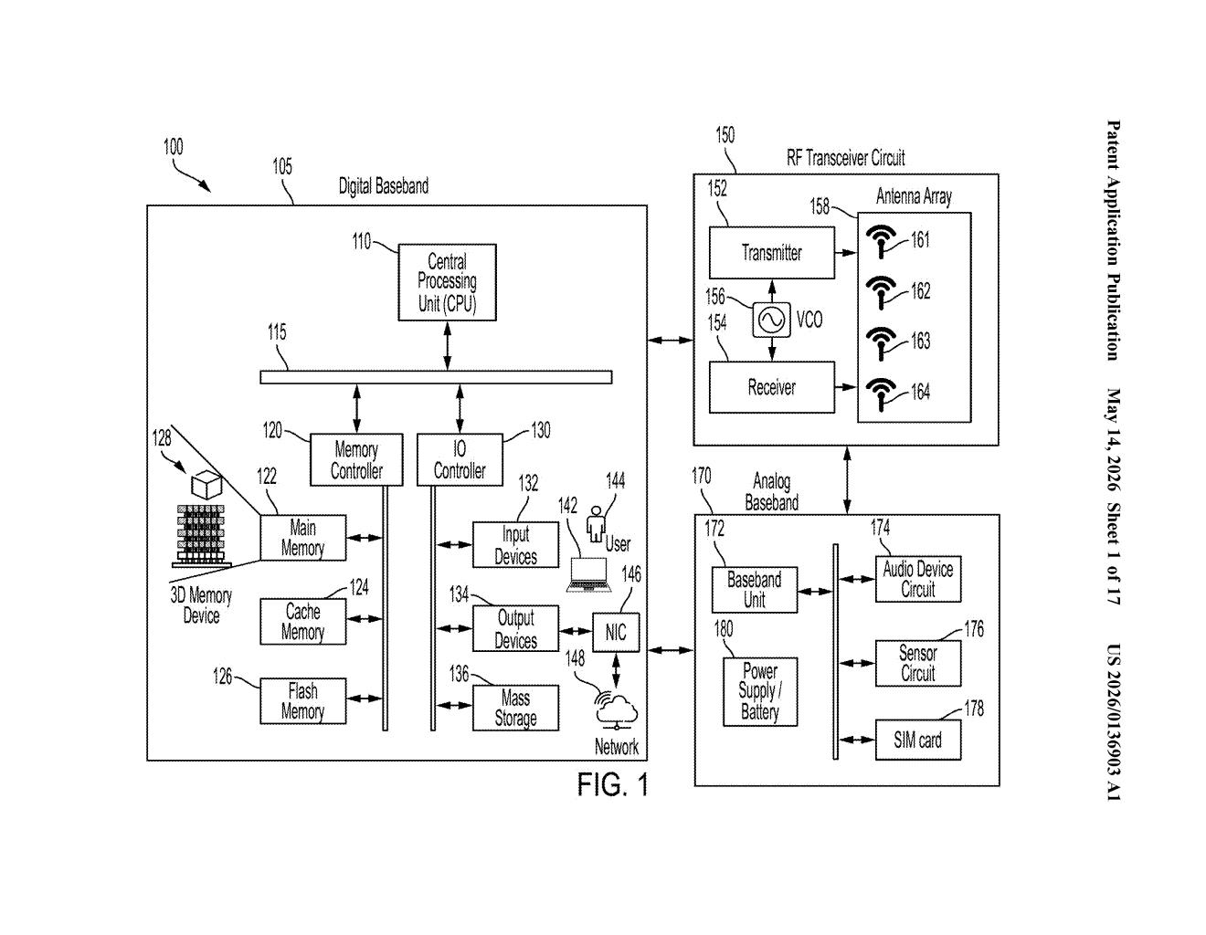
Imagine a skyscraper where every floor needs its own dedicated elevator shaft to the ground. In 3D NAND memory chips, something similar happens — each layer of memory cells has a wordline (a row of cells) that needs a metal contact point reaching down to the chip's control circuitry. As manufacturers stack more layers, managing all those contact points gets very crowded.
Samsung's patent describes a structured way to arrange contact pads — the small metal landing zones where electrical connections meet the wordlines — so that pads for different wordlines line up neatly in a specific direction, even when the wordlines themselves are at varying distances from their contact points. Think of it like staggering the elevator doors on alternate floors so they don't all collide in the same shaft.
The goal is cleaner, more predictable wiring geometry that lets you pack more memory layers into the same chip footprint without the contacts getting in each other's way.
How the offset pad alignment connects stacked wordlines
The patent describes a contact pad structure used to electrically connect wordlines — the horizontal row conductors inside a 3D memory array — to the peripheral circuitry that drives them.
The key idea is a two-pad arrangement:
- A first pad sits on a first contact point and connects via a routed conductor to a first wordline that runs lengthwise in one direction, but sits at a specific distance away from that contact point.
- A second pad does the same for a second wordline, which may be at a different distance from its own contact point.
- Both pads are aligned along a second direction (perpendicular to the wordlines), based on where the contact points are located — not based on where the wordlines themselves terminate.
The alignment-by-contact-point approach matters because in a staircase-style 3D memory structure (think of the layered terraces used in 3D NAND), wordlines at different heights have their endpoints staggered. By anchoring the pad alignment to the contact points rather than the wordline ends, the layout remains orderly even as the wordline-to-contact distances vary across layers.
This is fundamentally a back-end-of-line (BEOL) interconnect geometry — the metal wiring layers fabricated after the memory cell stack itself is built.
What this means for next-gen NAND flash density
3D NAND flash is in a relentless race to add more layers — Samsung, SK Hynix, and Micron are all pushing past 200+ layers. Every additional layer means more wordline contact pads competing for the same peripheral area around the memory array. Inefficient pad layouts waste chip area, which directly limits how much memory you can fit on a given die size and drives up cost per gigabyte.
For you as a consumer, tighter pad geometry contributes to cheaper, denser SSDs and smartphone storage over time. For Samsung as a manufacturer, a cleaner contact pad scheme can simplify the lithography steps needed to define those connections, potentially improving yield and reducing the number of fabrication masks required — both of which matter enormously at volume.
This is deep semiconductor process engineering — the kind of unglamorous layout patent that nobody tweets about but that quietly determines whether a 300-layer NAND chip is manufacturable at a reasonable yield. It's not a flashy AI or device patent, but for anyone tracking Samsung's NAND competitiveness against SK Hynix and Micron, this is exactly the kind of incremental interconnect work that adds up. Worth a bookmark if you follow memory chip manufacturing.
Get one Big Tech patent every Sunday
Plain English, intelligent commentary, no hype. Free.
Editorial commentary on a publicly published patent application. Not legal advice.