IBM Patents a Transistor-Swapping Trick to Shrink Chip Cell Layouts
IBM has found a clever workaround for a rigid constraint in chip layout tools — temporarily disguising one type of transistor as another so an automated layout engine places it more efficiently, then swapping it back.
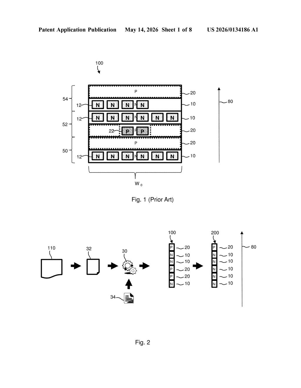
What IBM's transistor-swapping layout trick actually does
Imagine you're packing a suitcase and the organizer only lets you put shoes in the left half and clothes on the right. But what if one shoe would actually fit better on the right side? IBM's patent is essentially a hack for that exact problem — but for microchips.
In chip design, standard cell layouts alternate between two flavors of transistors — think of them as NMOS (one type) and PMOS (another type) — in fixed lanes. Automated layout tools strictly respect these lanes, which can leave wasted space.
IBM's method briefly disguises certain transistors as the other type, lets the layout tool place them optimally in the "wrong" lane, then converts them back and adapts the surrounding region to match. The result is a more compact chip layout without rewriting the underlying layout tool itself.
How IBM's type-swap method fools the layout generator
The patent describes a software method that slots into an existing standard cell layout generation workflow — the automated process chip designers use to turn a circuit schematic into a physical arrangement of transistors on silicon.
Normally, layout tools enforce strict alternating rows: PMOS transistors (field effect transistors of the first type, which use holes as charge carriers) go in their dedicated rows, and NMOS transistors (field effect transistors of the second type, which use electrons) go in theirs. This rigidity can prevent optimal packing.
IBM's method introduces a pre-processing and post-processing wrapper around a standard layout engine:
- Pre-processing: Identify which PMOS transistors could be better placed in an NMOS row, then temporarily relabel them as NMOS in the netlist (the file describing circuit connections).
- Layout run: Feed the modified netlist into an unmodified standard cell layout generator, which now places those disguised transistors in the NMOS region.
- Post-processing: Translate the temporary NMOS transistors back to PMOS, and adapt the local well region — the physical doping area in the silicon — to be the correct type.
The key insight is that the surrounding silicon region (called a well) also gets retyped, so the final layout is physically valid — not just a labeling trick.
What this means for chip density and EDA tooling
For chip designers, cell density is everything — more logic per square millimeter means cheaper, faster, lower-power chips. EDA (electronic design automation) tools are notoriously hard to modify, so finding ways to get better results without changing the core tool is genuinely valuable engineering. This approach works as a pre/post wrapper, meaning it could theoretically be added to existing design flows without massive retooling.
The technique is particularly relevant as the industry pushes toward complementary FET (CFET) and other advanced transistor architectures where NMOS and PMOS devices are stacked vertically — blurring the strict row separation this trick exploits. IBM's position in advanced logic research makes this a plausible building block for next-generation cell compaction methods.
This is a solid, practical EDA patent — not a moonshot, but the kind of unglamorous plumbing work that actually ships in design tools. The type-swap-and-restore approach is elegant in its simplicity: it sidesteps the need to modify expensive, mature layout generators by wrapping them in smarter pre/post logic. IBM's chip design software heritage makes this a credible filing.
Get one Big Tech patent every Sunday
Plain English, intelligent commentary, no hype. Free.
Editorial commentary on a publicly published patent application. Not legal advice.