
Samsung Patents a Camera Sensor That Handles Bright and Dark Areas Simultaneously
Samsung has patented a camera sensor pixel with two separate electrical pathways for moving charge off a light-catching element, a design that could give future sensors more flexibility in handling bright highlights and dark shadows at the same time.
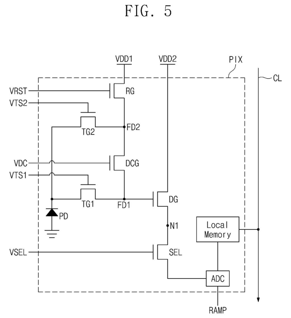
What Samsung's two-path image sensor pixel actually does
Imagine you are photographing a sunset: the bright sky goes white and the shaded ground goes pitch black in the same shot. That is the classic problem every phone camera wrestles with. It comes down to how the tiny chip inside the camera handles very bright and very dim light at the same time.
Samsung's patent describes a pixel built with two separate routes for moving the tiny burst of electricity that light creates when it hits the chip. A single light-catching speck can send that burst down either route, controlled by two independent switches. A third switch can connect the two routes, giving the chip extra control over how much of that electricity it collects and how strongly it reacts to the incoming light.
Having two exits instead of one means the chip can, in a single moment, act like a very alert sensor for dark areas while also acting like a calmer, less easily overwhelmed sensor for bright areas. The pixel does not need to be physically bigger to do this. That flexibility is what lets a camera hold detail in both the bright sky and the dark foreground.
a photodiode configured to accumulate charges based on an optical signal; a first transfer transistor connected between the photodiode and a first floating diffusion node …
Translation: This part captures light and sends the resulting electrical charge to a specific storage point.
How the dual floating-diffusion circuit routes light data
The patent centers on a pixel circuit with one photodiode and seven transistors arranged around two distinct storage nodes called floating diffusion nodes (think of them as tiny charge buckets, one on each side of the pixel).
- A first transfer transistor moves charge from the photodiode into the first bucket.
- A second transfer transistor routes charge to the second bucket instead.
- A dual conversion transistor sits between the two buckets and can link or isolate them on demand.
- A reset transistor, a drive transistor, and a select transistor handle clearing, amplifying, and reading the stored charge out to the rest of the chip.
The key variable is conversion gain: essentially how large a voltage swing the sensor produces per unit of collected light. By bridging or separating the two floating diffusion nodes with the dual conversion transistor, the circuit can switch between high-gain mode (good for low light) and low-gain mode (good for bright scenes) within a single pixel.
The drive transistor reads the voltage on the first floating diffusion node specifically, and the output travels through the select transistor onto a shared column line that feeds the rest of the imaging pipeline. The architecture keeps the readout path short, which helps reduce noise in the final signal.
… a dual conversion transistor connected between the first floating diffusion node and the second floating diffusion node, and operating based on a dual conversion signal …
Translation: This component links two storage areas to help the sensor manage varying light levels.
What this means for Samsung camera sensors going forward
Dynamic range is arguably the single most important quality metric for a smartphone camera sensor right now, and this kind of dual-path pixel architecture is one of the main ways chip designers try to improve it without simply making pixels larger (which would require a bigger, more expensive sensor die). Samsung's chip division supplies image sensors to its own Galaxy phones as well as other device makers, so a refinement here could ripple across a wide range of products.
The design is incremental rather than a departure from existing sensor architecture; similar dual-conversion-gain ideas have been explored across the industry. What patents like this one represent is the steady, component-level engineering that makes each sensor generation slightly better than the last, and that steady work is the kind of interesting tech patents in the image-sensor space that rarely make headlines but shape what your phone camera can actually see.
Samsung's 88th filing we've tracked since May in our camera sensor work builds on earlier applications like one blocking edge blur and one combining video and motion.
The underlying hardware this patent describes is already made in factories today. That means Samsung is not starting from scratch, and a real product could arrive soon.
The main work left is proving this exact circuit setup actually cuts noise or handles bright and dark scenes better than what is shipping now. That is a testing and fine-tuning problem, not a moonshot. Samsung is clearly adjusting its camera sensors at a fine level, with a credible shot at a phone that simply takes better photos in difficult light.
There are more where this came from
We read every patent application Big Tech publishes and send you the ones worth knowing. Plain English, free, every week.
The drawings
15 drawing sheets from US 2026/0243599 A1 · click any drawing to enlarge


Want this weekly breakdown for a company we don't cover? Patentlyze Pro →
Be the first to weigh in