
Samsung Patents an Image Sensor Design That Bridges Pixel Charge-Storage Regions
Every pixel in a digital camera has a tiny charge-storage pocket, and electrical interference in that pocket is one of the main reasons low-light photos look grainy. Samsung's new patent targets exactly that pocket with a new structural approach.
What Samsung's pixel charge-storage fix actually does
A street photographer shoots a dimly lit alley at night. The camera's sensor struggles, and the final image comes back speckled with noise. That noise often starts deep inside individual pixels, where electrical charge is stored before being read out.
Your phone camera's sensor is packed with millions of these pixel "charge pockets," called floating diffusion regions. They sit next to insulating walls that separate one pixel from another. The problem is that those walls and pockets can create unwanted electrical effects that corrupt the signal before it even becomes a photo.
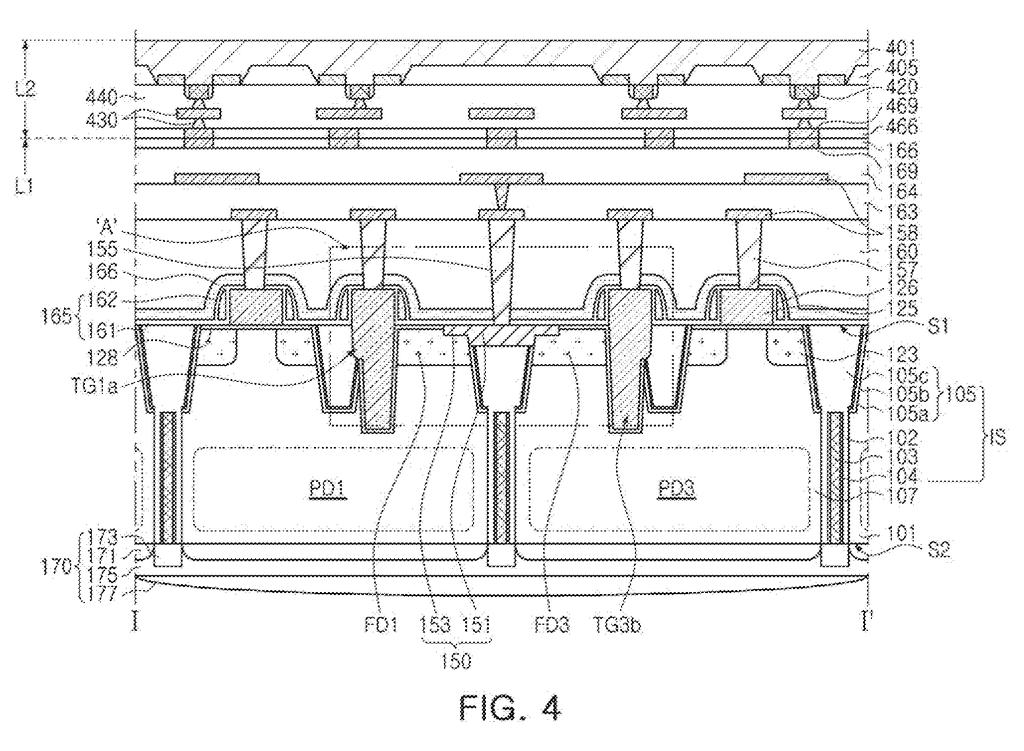
Samsung's patent describes a conductive structure that sticks up vertically from the surface of both the insulating wall and the charge pocket at the same time, physically connecting them. The idea is that by tying those two structures together with a conductor, you can control how charge behaves at that boundary and reduce the interference that causes noise.
… a floating diffusion region in a pixel region of the pixel regions, the floating diffusion region being configured to store charge transmitted from a photoelectric conversion region …
Translation: This area holds the electrical charge generated when light hits the sensor.
How the conductive structure connects the two regions
Samsung's patent describes an image sensor with a specific structural addition at the level of individual pixels.
Each pixel on an image sensor contains a photoelectric conversion region (the part that turns incoming light into electrical charge) and a floating diffusion region (a tiny reservoir that temporarily holds that charge before it gets measured). Sitting right next to the floating diffusion region is an element isolation region, essentially an insulating fence that keeps neighboring pixels from electrically contaminating each other.
The patent's key addition is a conductive structure that protrudes vertically upward from the surfaces of both the isolation region and the floating diffusion region simultaneously, physically contacting and bridging both. Think of it as a narrow metal fin that stands up from the border between two adjacent zones.
The claim is precise about geometry: the fin starts at the "first surface" (think: top) of both regions and extends down toward their opposite surfaces, making contact with both along the way. This controlled electrical connection at that boundary is the core of what Samsung is protecting here.
… a conductive structure protruding in a vertical direction from a first surface of the element isolation region and a first surface of the floating diffusion region …
Translation: A vertical metal bridge connects the components to manage the stored electrical charges.
What this means for camera sensor noise levels
The floating diffusion region is one of the most noise-sensitive spots in any image sensor. Any stray charge or voltage instability at the boundary between that region and the isolation wall gets amplified into the final signal, showing up as grain or color error in your photos. A structural approach that physically stabilizes that boundary at the semiconductor level could reduce that noise source without requiring more processing after the fact.
For Samsung, which supplies image sensors to a broad range of smartphone and camera makers, incremental improvements in pixel-level architecture compound across billions of devices. This particular filing sits squarely in the chip design corner of Big Tech patent news, where image sensor architecture patents have been a steady and competitive category across major semiconductor players.
This is the 95th Samsung filing we've tracked since May in our camera sensor push watch, joining one on flicker detection and one on per-shot data storage.
The problem this patent targets is real. Floating diffusion noise is a well-documented limit in image sensor performance, and it matters most in exactly the conditions that are hardest for cameras: low light, fast scenes, small pixel pitch. The problem does not get smaller as sensors scale down; it tends to get worse as pixels get physically tinier and more tightly packed.
The structural solution here is narrow in scope. It does not propose a new pixel architecture or a new material. It describes a specific geometric connection between two adjacent regions, which is the kind of incremental claim that characterizes mature, competitive chip design. That is not a criticism; at this stage of image sensor development, the gains come from details exactly this small.
Whether this specific conductive bridge delivers a measurable improvement in real-world noise performance depends on fabrication details the patent does not spell out. The concept is plausible, the problem is genuine, and the approach is tightly matched to the scale of the issue rather than overstated.
Get our take in your Top Stories
Liked this breakdown? Add Patentlyze as a preferred source on Google, and our plain-English take shows up more often in your Top Stories the next time Samsung patent news breaks.
There are more where this came from
We read every patent application Big Tech publishes and send you the ones worth knowing. Plain English, free, every week.
The drawings
32 drawing sheets from US 2026/0255713 A1 · click any drawing to enlarge


Want this weekly breakdown for a company we don't cover? Patentlyze Pro →
Be the first to weigh in