
Samsung Patents a Camera Chip Design That Stops Unwanted Light From Blurring Edges
Stray light sneaking in at the edges of an image sensor is one of the quieter reasons photos look washed out or hazy. Samsung's latest patent tackles that problem with a two-layer barrier built right into the sensor itself.
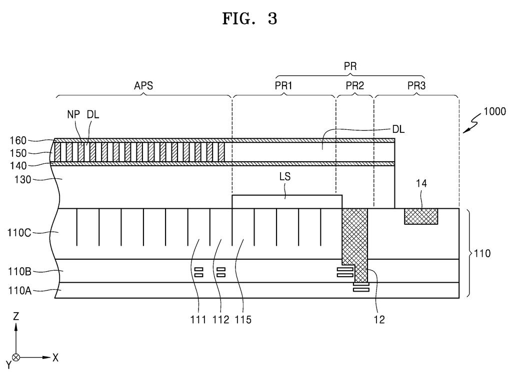
How Samsung's sensor edge stops light from ruining your photos
Camera sensors have an edge problem. Light that hits the border of a sensor instead of the active pixel area can bounce around and create a haze or glow that softens an otherwise sharp image. This is a known limitation of how image sensors are built, and it gets harder to manage as sensors shrink.
Samsung's patent describes a sensor that places a special two-part shield along that border region. One layer reflects stray light back away from the sensor, and a second layer absorbs whatever gets through, using an inorganic (non-organic, mineral-based) material that holds up well over time.
The active picture-taking area of the sensor also uses tiny structures called nanostructures, positioned just above the pixel layer, to better direct light where it belongs. Together, these features are designed to keep light well-behaved across the whole sensor, which could translate into cleaner, more consistent images straight out of your phone's camera.
… the periphery region comprises a light-shielding layer disposed on the sensor substrate and at the edge of the active pixel sensor region, and the light-shielding layer comprises a light-reflective layer and a light-absorbing layer comprising an inorganic material.
Translation: The sensor uses a special border coating made of reflective and light-absorbing materials to block stray light at the edges.
How the reflective and absorbing layers work together
The patent describes an image sensor split into two functional zones: an active pixel sensor region (the area that actually captures image data) and a periphery region (the border strip around the edge).
In the active zone, the sensor uses a layer of nanostructures, tiny engineered features spaced just above the pixel substrate. These act like microscopic light guides, helping incoming light hit pixels at the right angle rather than scattering.
The periphery region gets a different treatment: a light-shielding layer made of two sub-layers stacked together:
- Light-reflective layer: bounces stray light away before it can reach the pixels
- Light-absorbing layer: catches any light the reflective layer misses, using an inorganic material (think ceramics or metal compounds rather than plastics or polymers) that resists degradation
The key engineering insight is that a single shielding approach, either reflection or absorption alone, leaves residual stray light. By combining both in a defined order at the sensor edge, Samsung aims to suppress the light leakage that causes image artifacts like halation (a glow around bright areas) or reduced contrast near the frame's border.
The active pixel sensor region may include a plurality of nanostructures disposed to face the sensor substrate and spaced apart from the sensor substrate …
Translation: The sensor features tiny structures that hover slightly above the main surface to help capture light more effectively.
What this means for Samsung camera quality
For anyone who has noticed that photos shot against a bright window or a streetlight at night sometimes look soft or glowy around the edges, this is the kind of sensor-level fix that addresses that. Better stray-light suppression means more of the image area can be used reliably, and the edges of photos stay as sharp and accurate as the center.
This is a component-level filing, so it speaks to Samsung's ongoing work on the image sensor hardware it supplies to its own Galaxy phones and to other manufacturers. Samsung's sensor division (ISOCELL) is a major supplier across the Android ecosystem, meaning improvements like this can ripple well beyond Samsung-branded devices. Image sensor engineering is one of the steadier areas covered among the newest Big Tech patents, reflecting how competitive the camera hardware space remains even as software processing gets most of the attention.
Most people never think about image sensor edges, but photographers who have compared shots from different phone cameras often feel the difference as a vague sense that one camera's images just look "cleaner." Samsung is targeting exactly that subtle quality gap with a structural fix rather than a software workaround, which suggests more durable and consistent results across varied lighting. If this design reaches production sensors, the payoff shows up in every photo taken in backlit or high-contrast scenes, which is precisely when cameras tend to disappoint.
There are more where this came from
We read every patent application Big Tech publishes and send you the ones worth knowing. Plain English, free, every week.
The drawings
14 drawing sheets from US 2026/0239758 A1 · click any drawing to enlarge


Want this weekly breakdown for a company we don't cover? Patentlyze Pro →
Be the first to weigh in