
Samsung Patents a Display That Adjusts Power Voltage Region by Region
Samsung is patenting a display technique that feeds different power levels to different parts of the screen at the same time, then adjusts those levels between frames to reduce wasted energy.
What Samsung's split-voltage screen actually does
Imagine your phone screen is showing a dark menu on the left side and a bright photo on the right. Right now, most screens apply the same power voltage across the entire panel, even though bright areas and dark areas need very different amounts of energy. That means the dark side is being fed more power than it needs, and that extra power just turns into heat.
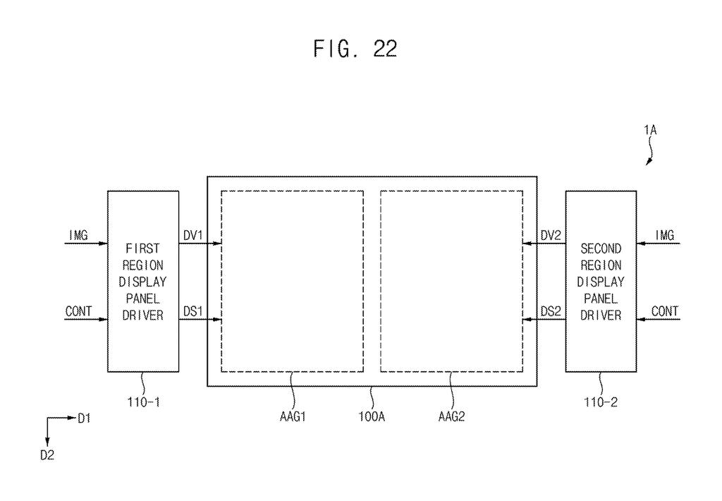
Samsung's patent describes a display that splits the screen into at least two regions and gives each one its own power supply voltage. The bright region gets a higher voltage; the darker region gets a lower one. The key detail is when that voltage change happens: between the moments pixels are actively lit, during what the patent calls the "non-emitting period." Changing voltage while the pixels are dark avoids the kind of visual flicker you'd otherwise see.
The result, in theory, is a display that wastes less power by matching the energy it delivers to the content actually on screen. For phones and tablets, that could translate to a bit more battery life without touching the screen itself.
… a first high power voltage applied to the first display region is different from a second high power voltage applied to the second display region, and wherein a voltage level of at least one of the first high power voltage or the second high power voltage is changed in the non-emitting period.
Translation: The screen can adjust the power levels for different sections of the display even while the pixels are turned off.
How the voltage shifts happen between frames
Every pixel in an OLED or similar display has a small circuit driving it. That circuit takes a high power voltage (think of it as the pressure behind the electrical current) and uses it to push the right amount of current through the light-emitting element. More voltage headroom generally means brighter pixels, but it also means more power consumed even when you don't need full brightness.
This patent splits the display panel into a first display region and a second display region, each with its own independently adjustable high power voltage. If the content on one side of the screen is darker, its voltage can be dropped; the other side keeps a higher voltage for brighter content. The two voltages can be different at the same time.
The clever constraint is when the voltage is allowed to change. A display frame has two phases:
- Emitting period: pixels are lit and visible to the viewer
- Non-emitting period: pixels are temporarily off while the next frame is being written
The patent specifies that voltage adjustments happen only during the non-emitting period. Changing voltage while pixels are dark prevents the shift from showing up as a visible brightness glitch or flicker.
The display panel driver coordinates both the per-region voltages and the timing so that the transition always lands inside that dark window.
A pixel circuit included in the display panel may include a writing transistor, a driving transistor configured to generate a driving current based on a high power voltage and a light emitting element configured to receive the driving current.
Translation: Each individual pixel contains a set of transistors that control how much electricity flows to the light source.
What this means for OLED power efficiency
For OLED displays, power consumption tracks closely with what's on screen. A phone showing a dark wallpaper burns far less battery than one showing a white document. This patent pushes that logic further by letting the power rail itself respond to content at a sub-screen level, rather than treating the whole panel as a single load. That matters most for devices with mixed-content screens: a tablet split between a video and a notes panel, or a phone with a persistent status bar.
The efficiency gain is real but incremental. Samsung is essentially fine-tuning a knob that already exists (the supply voltage) rather than introducing a new kind of pixel technology. Still, in a market where display power is one of the biggest drains on battery life, incremental counts. Display-power patents like this one are among the interesting tech patents showing how much engineering effort the industry puts into squeezing efficiency from OLED panels without changing what users actually see.
Samsung's 82nd filing we've tracked in our Samsung display technology work since May builds on earlier applications like one on ink-spreading blades and one on per-color pixel voltage.
There is a real tradeoff here. Splitting the screen into separately powered zones means extra hardware and precise timing to keep everything in sync. Get the timing wrong, even slightly, and you see visual glitches.
Samsung is betting that modern chips can handle that coordination reliably enough to make the power savings worth the extra parts. That bet makes sense for expensive, high-end screens. Budget phones will likely never see this feature.
There are more where this came from
We read every patent application Big Tech publishes and send you the ones worth knowing. Plain English, free, every week.
The drawings
18 drawing sheets from US 2026/0245499 A1 · click any drawing to enlarge


Want this weekly breakdown for a company we don't cover? Patentlyze Pro →
Be the first to weigh in