
Samsung Patents a Laser System for Placing Tiny LEDs on Curved Screens
Building a screen out of millions of microscopic LEDs is painstaking work, and placing them on anything other than a flat rectangle makes it far harder. Samsung's latest patent describes a laser-guided system that can handle both problems at once.
What Samsung's micro-LED laser transfer actually does
Ever tried to pick up a single grain of rice with tweezers and drop it exactly where you want it, a million times in a row? That is roughly the challenge Samsung is solving here, except the grains of rice are LEDs smaller than a human hair.
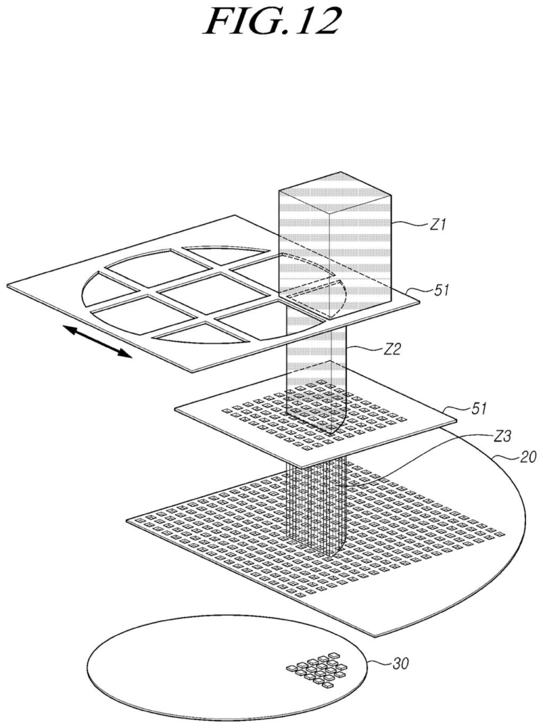
Modern micro-LED displays are built by transferring vast numbers of those tiny light sources from a source tray onto the final screen. Samsung's patented system uses a laser beam plus a programmable mask (think of it as a stencil with holes that open and close on command) to fire only the LEDs you actually need. If a spot on the destination screen is already filled, the mask blocks the laser for that position. If the screen has an unusual shape, like a curved watch face or a non-rectangular car display, the system adapts its pattern accordingly.
The filing also describes a backup transfer device that can step in when the first one finishes or runs into trouble, keeping the process moving without manual intervention.
… a processor, including a processing circuit, to control the mask unit to open and close the at least one aperture corresponding to the micro LED transferred to the second substrate …
Translation: A computer chip manages a shutter system to precisely place individual tiny LEDs onto the screen surface.
How the mask controls which LEDs get fired and where
The patent covers a micro-LED transfer system with two coordinated transfer devices. The core of the first device is a trio of components working together:
- Laser light source: fires a beam at a "donor" substrate (the starting tray) where thousands of micro-LEDs sit waiting to be moved.
- Mask unit: sits between the laser and the substrate and contains apertures (small openings) that a processor can open or close individually, acting as a physical filter that lets the laser through only where a new LED is needed.
- Processor: tracks which positions on the destination screen are already populated and instructs the mask to skip those spots, preventing double-placement and waste.
The second transfer device functions as a parallel or backup tool. The patent specifies that at least one of the two devices must be able to deposit LEDs onto a substrate with an irregular shape, meaning non-flat, non-rectangular surfaces like curved panels or uniquely contoured wearable displays.
The selective-opening mask is the key differentiator here. Without it, a laser would indiscriminately lift every LED in its path. With it, the system can place individual LEDs with surgical precision while skipping ones already in place, which is essential when repairing or partially re-manufacturing a display.
The first transfer device and/or the second transfer device can transfer the micro-LED to the second substrate, which has an irregular shape.
Translation: The machine is designed to place these tiny lights onto curved or uneven surfaces rather than just flat glass.
What this means for curved and custom-shaped displays
Micro-LED displays are widely considered the next step up from OLED, promising brighter images, longer lifespans, and lower power draw. The manufacturing bottleneck has always been the transfer step: moving millions of near-invisible chips accurately and quickly enough to be economically viable. A system that can skip already-placed LEDs and adapt to curved or non-standard screen shapes would address two of the hardest parts of that bottleneck at once.
For consumers, this kind of manufacturing progress is what eventually brings premium display technology into everyday products, whether that means a watch with a wrap-around screen or a car dashboard that curves across the full width of the cabin. Samsung's display division is one of the few operations in the world with the scale to actually industrialize micro-LED production, making filings like this one worth tracking alongside the broader stream of plain-English patent summaries covering display and semiconductor manufacturing.
Samsung's 83rd filing we've tracked since May in our display technology work, following one on region-by-region power voltage and one on ink-spreading blades, adds another piece to how screens are designed.
Getting this technology into real products will not be easy. The patent describes a set of specialized factory machines that all have to be built, tuned, and connected before a single screen benefits. That puts it squarely in the "factory plumbing" category, far from anything a shopper will touch soon.
What the document does make clear is that Samsung is pouring serious engineering effort into cutting waste and making screens in more shapes. That is exactly where the real fight over premium displays will play out over the next several years.
There are more where this came from
We read every patent application Big Tech publishes and send you the ones worth knowing. Plain English, free, every week.
The drawings
15 drawing sheets from US 2026/0247769 A1 · click any drawing to enlarge


Want this weekly breakdown for a company we don't cover? Patentlyze Pro →
Be the first to weigh in