
Qualcomm Patents a New Chip Design That Runs Multiple AI Calculations at Once
AI models are hungry for math, and doing that math one step at a time is slow. Qualcomm's latest patent describes a chip design that bundles many calculations together and fires them off simultaneously, which is exactly what on-device AI needs.
What Qualcomm's parallel AI chip approach actually does
Ever wondered why some phones handle AI tasks effortlessly while others stutter? The short answer is the chip inside, specifically how efficiently it crunches numbers.
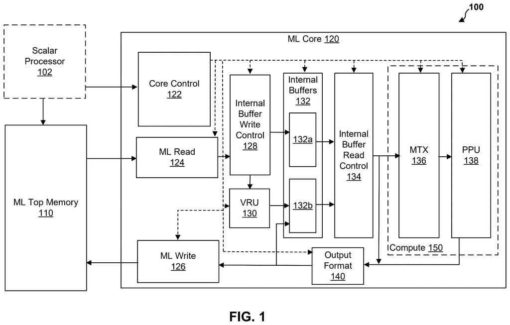
AI models work by running huge tables of numbers (called matrices) through mountains of arithmetic. Qualcomm's patent describes a chip that accepts a single instruction covering many rows of data at once, instead of plodding through one row at a time. Think of it like asking a crew to paint a room together rather than having one person do every wall in sequence. The chip's controller receives that bundled instruction, a buffer area collects the incoming data, a compute block does the actual math across all the rows in parallel, and then a formatting block packages the result.
The goal is getting more AI work done per second without burning extra battery, which matters a lot if you want features like real-time translation or photo enhancement running on your phone rather than in a distant data center.
a core controller configured to receive a multi-vector instruction for a first operation on a matrix, the instruction indicating a vector length and a number of vectors …
Translation: The main control unit takes in complex math instructions that specify the size and amount of data to process.
How the accelerator processes multiple vectors at once
The patent describes a hardware accelerator (a chip or chip section dedicated solely to AI math) that introduces a new instruction type called a multi-vector instruction.
Normally, a chip instruction says: "do operation X on this one vector" (a vector being a single row or column of numbers). A multi-vector instruction says: "do operation X on this many vectors, each of this length" in one go. That single command carries enough information to keep the whole compute block busy without waiting for follow-up instructions.
The accelerator has four main parts working together:
- Core controller: receives the multi-vector instruction and figures out how many rows to process and how long each one is.
- Write control block: loads the matrix data into an on-chip buffer, keeping the compute unit fed with numbers.
- Compute block: executes the requested operation (addition, multiplication, activation functions, etc.) across every vector in the batch simultaneously.
- Output format block: arranges the results in whatever shape downstream layers of the AI model expect.
The key engineering bet is that defining vector count and vector length inside the instruction itself (rather than in separate control logic) lets the chip adapt to different AI model shapes without needing entirely different hardware for each one.
… a compute block configured to perform the operation indicated by the multi-vector instruction on each of the number of vectors …
Translation: The processing engine carries out the requested math operations across multiple data streams at the same time.
What this means for AI chips in phones and devices
Most of the AI features phone makers advertise, from live caption to on-camera photo editing, run on a dedicated AI chip block. The bottleneck is rarely raw transistor count; it is how efficiently the chip keeps its compute units busy rather than sitting idle waiting for instructions. the pattern in Qualcomm's AI silicon filings points toward closing that gap at the instruction level, which is a lower-level fix than adding more cores.
For you, the practical upshot is faster AI responses and lower battery drain on Snapdragon-powered phones and laptops. For chip designers, it means fewer instructions needed to describe a workload, which cuts the overhead that currently chews through power budgets on every AI inference.
Qualcomm's 53rd filing we've tracked since July in the AI chip wars watchlist continues a pattern seen in one on ordered calculations and one on controlled chip tasks.
AI chips spend a surprising amount of their time on housekeeping: reading instructions, understanding what each one means, and fetching the right numbers before any real math happens. At the scale of a modern AI model, that overhead accumulates into a real cost, measured in slower responses and higher electricity bills.
The problem Qualcomm is attacking here is structural. Because AI workloads repeat the same types of calculations millions of times, issuing one broad instruction that covers a whole block of related work cuts the housekeeping proportionally. The approach is well-matched to the size of the waste it targets.
How much of that benefit reaches everyday products depends on the software that translates AI models into chip instructions. If that software learns to take full advantage of these broader instructions, the gains in speed and efficiency become real for users. If it does not, the hardware sits waiting.
There are more where this came from
We read every patent application Big Tech publishes and send you the ones worth knowing. Plain English, free, every week.
The drawings
4 drawing sheets from US 2026/0277605 A1 · click any drawing to enlarge


Want this weekly breakdown for a company we don't cover? Patentlyze Pro →