Qualcomm
Qualcomm · Chip · Filed Feb 20, 2025 · USPTO published Aug 20, 2026 · Aug 20 release
Qualcomm Patents a Way to Let Memory Chips Handle Multiple Jobs at Once
Qualcomm is patenting a way for memory chips to pause one job, save its place, and switch to another without losing any work, much like a computer's operating system does for software, but built directly into hardware.
- Publication number
- US 2026/0244482 A1(US20260244482A1)
- Applicant
- QUALCOMM Incorporated
- Filed · Published
- Feb 20, 2025 · Aug 20, 2026
- Inventors
- Subbarao Palacharla, Pan Deng, Rui Cao, Pankaj Deshmukh, Jungwon Suh
- Status when we published
- Examiner raised objections; the company can respond
- Document
- 20 claims
- US classification
- 712/228
- Examiner
- ABAD, FARLEY J (Art Unit 2181)
How Qualcomm's in-memory multitasking actually works
Every time your phone runs a navigation app, plays music, and checks your email at the same time, several processors are competing for the same memory. That memory has to serve all of them without dropping the ball.
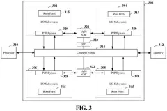
Qualcomm's patent describes a system where the memory chip itself acts as a kind of traffic coordinator. When one processor's task gets interrupted, the chip saves a snapshot of exactly where that task was, tucks it away inside the memory bank, and lets another processor's task run. When it's time to return, the chip pulls that snapshot back out and picks up right where things left off.
The goal is to stop processors from stepping on each other's work when they all share the same physical memory. Instead of each processor managing this juggling act on its own, the memory chip handles it internally, which could make the whole system faster and less wasteful.
… saving, by the memory controller, the first PIM context associated with the interrupted execution of the first task to a memory bank of the PIM device; and restoring, by the memory controller using the first PIM context saved to the memory bank, execution of the first task on the first virtual PIM.
Translation: The memory controller saves the current state of a paused task directly into the memory chip so it can resume later.
How the memory controller saves and restores each task's state
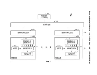
The patent covers a processing-in-memory (PIM) device, which is a chip that can do some computing work inside the memory itself rather than shipping data back and forth to a separate processor. That round-trip normally eats up time and power, so keeping computation local is a meaningful efficiency gain.
The twist here is multi-context support. A "context" in chip design means the complete saved state of a running task (think of it as a bookmark that captures every register value and in-progress calculation). Normally, if you have several processors sharing one PIM chip, they need to coordinate carefully so they don't overwrite each other's work.
Qualcomm's approach creates virtual PIMs (isolated slices of the physical chip, one per connected processor). Each processor thinks it has its own dedicated memory compute unit. The memory controller handles the reality:
- Interrupts a task when it's time to switch
- Receives the task's context from that processor
- Saves the context into a reserved memory bank on the chip
- Runs the next task from a different processor
- Restores the saved context and resumes the first task later
The context switching protocol (the rulebook that decides when and how to hand off) lives in the memory controller, keeping the connected processors largely unaware of the scheduling complexity underneath.
Systems, methods, devices, and apparatuses are disclosed for supporting and efficiently switching between multiple contexts associated with multiple system-on-a-chip (SoC) clients in a processing-in-memory (PIM) architecture.
Translation: This patent describes a way for memory chips to juggle tasks from several different processors at the same time.
What this means for chips running AI on a single device
On-device AI is pushing more and more processors onto a single chip package. Qualcomm's own Snapdragon platforms, for example, pack a CPU, GPU, and a dedicated AI engine onto one piece of silicon, and all of them want to read and write memory constantly. Without a coordination layer, they waste time waiting on each other or, worse, corrupt each other's in-progress work.
This patent puts that coordination inside the memory hardware rather than piling more software overhead onto each processor. For device makers building phones, laptops, or edge AI hardware, that distinction matters: software-based scheduling adds latency and burns battery, while a hardware solution handles it invisibly and faster. Engineers working on PIM architectures for inference accelerators will find this filing directly relevant, and it sits alongside a broader wave of new Big Tech patents targeting in-memory compute as the next front in the fight to shrink AI's power bill.
Qualcomm's 34th filing we've tracked since July in the AI chip wars space builds on one letting phones report AI capacity and one sharing memory processing across tasks.
Source: US 2026/0244482 A1 at the USPTO (PDF). Full patent text and figures are in the official publication.
Get our take in your Top Stories
Liked this breakdown? Add Patentlyze as a preferred source on Google, and our plain-English take shows up more often in your Top Stories the next time Qualcomm patent news breaks.
Add Patentlyze on Google
One click.
There are more where this came from
We read the new patents from Big Tech, carmakers and more and send you the ones worth knowing. Plain English, free, every week.
The drawings · 8 sheets
8 drawing sheets from US 2026/0244482 A1 · click any drawing to enlarge


More from Qualcomm
All 637 Qualcomm patents →
More in Chip
All 651 Chip patents →
Intel
Intel Patents a GPU Scheduling Trick That Stops Threads From Stepping on Each Other
Intel
Intel Patents a Processor That Bookmarks Its Own Memory Work Mid-Instruction
Samsung
Samsung Patents a Way to Decrypt Data Inside the Memory Chip Itself
Intel