
Samsung Patents a Nanostructure Lens That Splits Light Without Color Filters
Your phone camera wastes a surprising amount of the light it collects. Samsung is patenting a way to fix that by replacing the colored filters in image sensors with microscopic pillars that bend light directly onto the right pixels.
How Samsung's tiny pillars replace your camera's color filters
Every time you snap a photo in a dim room, your phone's camera is throwing away most of the light it catches. That happens because traditional sensors use tiny colored filters, one per pixel, that block every color except the one that pixel is supposed to record. Blocking light means a dimmer, noisier photo.
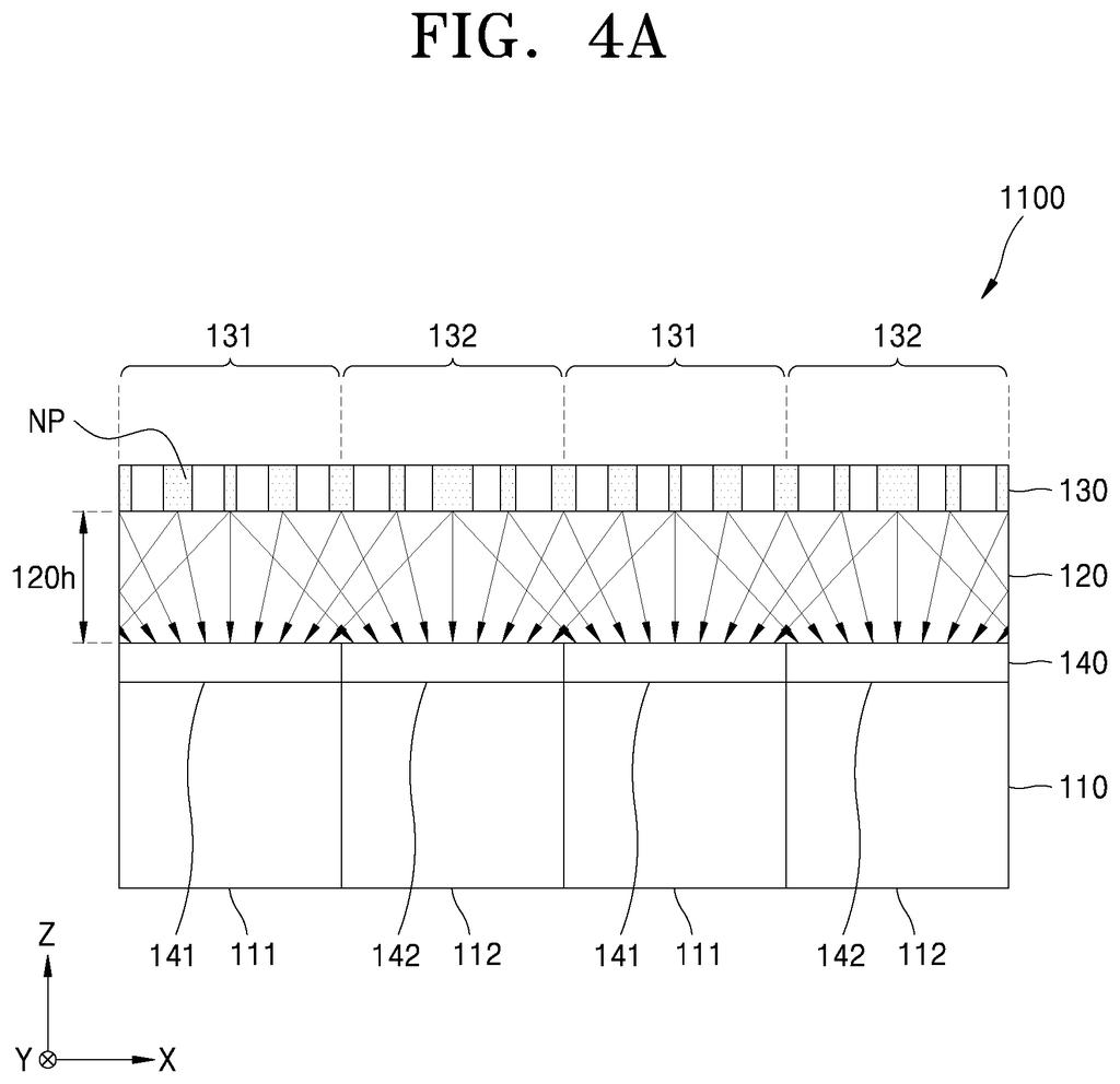
Samsung's patent describes a different approach: a grid of nanoscale pillars (called nanoposts) so small they sit at the level of individual wavelengths of light. Instead of blocking colors, these pillars bend light like a prism, steering red, green, and blue directly to the pixels that need them. Nothing gets wasted.
The clever part is that the pillars near the edges of the sensor don't look exactly like the ones in the center. Their shapes and widths shift depending on the angle of incoming light, so the whole array works correctly even when light hits the sensor at a slant rather than straight-on. That's the kind of precision tuning that could make future phone cameras noticeably better in low light.
… wherein widths of the first nanoposts of the first pixel corresponding regions in an area having an azimuth angle of 0 degree or 180 degrees change from a center portion of the color separating lens array to a periphery portion of the color separating lens array …
Translation: The size of the tiny pillars varies horizontally depending on how far they sit from the center of the lens.
How the nanoposts shift shape from center to edge
Traditional image sensors stack a colored filter directly over each pixel, a design called a Bayer filter array. Those filters absorb the colors they don't want, which is wasteful but simple to manufacture. The system in this patent replaces that filter layer with a color separating lens array (CSLA), a surface covered in nanoscale pillars made of a high-refractive-index material.
Each pillar, called a nanopost, is shorter than a single wavelength of visible light. By varying the shape, width, and arrangement of these posts, engineers can tune exactly which wavelengths get bent toward which underlying pixels. The sensor has four pixel types: two that collect the same primary color (boosting sensitivity for that channel), plus two others for the remaining primary colors. The nanoposts focus each wavelength onto its correct pixel type without absorbing anything.
The patent's specific contribution is how it handles the peripheral portion of the sensor. Light entering from the edges of a camera lens arrives at an angle rather than straight down. If the same nanopost geometry used in the center were applied to the edges, the color-sorting would degrade. Samsung's solution is to vary the widths of specific nanoposts across a key directional axis (azimuth 0/180 degrees) while keeping them constant along the perpendicular axis (azimuth 90/270 degrees).
This asymmetric correction compensates for the angled light without requiring a completely different nanopost design for every position on the chip, keeping the manufacturing problem tractable.
… at least one of a shape, a width, and an arrangement of the plurality of nanoposts of the plurality of first pixel corresponding regions changes according to an azimuth direction of the plurality of nanoposts in a peripheral portion surrounding a central portion of the color separating lens array …
Translation: The physical makeup of the nanostructures shifts around the edges of the lens to properly direct incoming light.
What filterless sensors could mean for phone cameras
For you as a phone user, the promise is photos with less noise in low light and sharper color reproduction, because more of the light the lens gathers actually reaches the sensor instead of being absorbed by a filter. Higher-end camera makers have chased filterless or filter-reduced sensor designs for years because the math on efficiency is compelling.
The engineering hurdle has always been the edge problem: a flat array of tiny structures that works beautifully in the center tends to fall apart near the edges where light arrives at steeper angles. Samsung keeps filing on nanostructure imaging suggests this is a sustained engineering push, not a one-off idea. Whether the manufacturing yield on a chip covered in billions of precisely shaped nanoposts is commercially viable at phone scale is the question this patent doesn't answer.
Samsung filed its 145th application we've tracked in our camera sensor push since May, building on work like cross-camera color consistency and selfie-assisted color correction.
The tiny light-steering pillars at the heart of this design are measured in nanometers, and when one goes wrong during manufacturing, it doesn't ruin a single pixel. It bleeds the wrong color across several neighboring ones, a steeper penalty than a smudged traditional filter, multiplied across the billions of pillars a single chip requires.
Samsung's answer to that fragility is to hold one dimension of the pillars constant and vary only the other, which narrows the manufacturing target but also means the design accepts incomplete correction for how light arrives at an angle. That's a real concession, not a footnote.
Whether the trade is worth it depends on who's buying. For a high-end camera where tighter tolerances are already baked into the price, the color accuracy gains likely earn their keep. For a mass-market phone sensor, the yield math probably doesn't close until the fabrication process improves considerably.
There are more where this came from
We read every patent application Big Tech publishes and send you the ones worth knowing. Plain English, free, every week.
The drawings
58 drawing sheets from US 2026/0299173 A1 · click any drawing to enlarge


Want this weekly breakdown for a company we don't cover? Patentlyze Pro →
Be the first to weigh in