
Samsung Patents a Camera Chip That Handles Autofocus and HDR Photography at Once
Most phone cameras have to choose between gathering focusing data and capturing a wide range of light in a single shot. Samsung is patenting a sensor design that does both at once, from the same set of pixels.
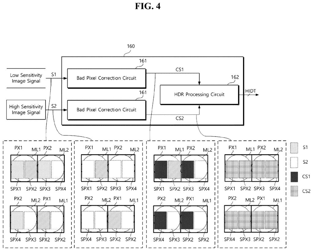
What Samsung's dual-output camera sensor actually does
A photographer points their phone at a dimly lit restaurant table scattered with candles and glasses. The camera needs to lock focus fast and keep detail in both the bright flames and the dark corners. Most sensors juggle these two jobs separately, which costs time and can introduce errors.
Samsung's patent describes a way to wire the tiny light-collecting cells inside a camera sensor so one readout produces two kinds of data simultaneously: phase data (which tells the camera how far out of focus the scene is) and HDR image data (which blends bright and dark exposures into one natural-looking picture).
Instead of dedicating separate pixels to each task, the design shares a single tiny lens across a cluster of sub-pixels, then routes the control signals for those sub-pixels through different internal wiring paths. That wiring difference is what lets the sensor pull double duty without adding bulk or sacrificing resolution.
… an image processing circuit configured to output high dynamic range (HDR) image data and phase data based on the plurality of image signals …
Translation: The chip processes signals simultaneously to produce both bright, balanced photos and autofocus data.
How the pixel wiring splits one sensor's job in two
The sensor is built around a pixel array where each pixel contains multiple sub-pixels that all share one microlens (the tiny dome of glass sitting on top of each light-gathering cell). Sharing a microlens is already common in phase-detection autofocus systems, where two sub-pixels sitting side by side see the scene from slightly different angles, and comparing their outputs tells the processor which way to move the lens to sharpen the image.
What makes this design different is in the wiring. Each sub-pixel has a transfer transistor, which is essentially a gate that controls when the collected light charge flows out to be measured. In a conventional sensor, sub-pixels at the same position in neighboring pixels are controlled by the same wire. Here, those same-position sub-pixels receive their control signals through different interconnections, meaning different wiring routes.
That wiring variation lets the image processing circuit read out the pixel signals in different combinations:
- Some readout patterns extract phase data, used for autofocus calculations.
- Other patterns extract HDR image data, combining exposures to preserve both highlight and shadow detail.
The readout circuit digitally converts all of these pixel signals, and the processing circuit then outputs both data types from a single capture cycle. The net effect is that autofocus and HDR imaging no longer have to take turns.
… sub-pixels sharing a microlens, each of the sub-pixels including a photoelectric element and a transfer transistor connecting the photoelectric element to a floating diffusion node …
Translation: Tiny light-gathering units beneath a shared lens each have their own microscopic switch and light detector.
What this means for smartphone camera performance
For you as a camera user, the practical payoff is fewer moments where the photo you actually wanted was lost to focusing delay or blown-out highlights. Phones already do a lot of computational work to stitch together HDR frames and hunt for focus, but doing those things sequentially means each step can go wrong independently. A sensor that gathers both types of data in one pass removes one of those failure points.
Samsung's track record in image sensor patents suggests this is part of a sustained push to move more of the camera's heavy lifting into the hardware itself, reducing reliance on software tricks. Whether this specific design reaches a shipping product, and when, depends on manufacturing considerations the patent doesn't address.
Samsung's 130th filing we've tracked since May in our camera sensor work watchlist follows a thinner zoom lens and a five-lens spacing design, each pushing tighter camera builds.
Faster focus and better exposure in the same shot, without changing how you shoot, is the real promise buried in this patent. A photo of a friend backlit by a bright window would show both the face and the sky clearly, and a moving subject would snap into focus without the camera hunting around first.
The engineering underneath is difficult to pull off across a full sensor at manufacturing scale, and the patent says nothing about yield or cost, which will decide whether this stays on paper or lands in a phone.
File this away for now. If Samsung makes it work, the benefit shows up in a future camera that simply gets more shots right.
There are more where this came from
We read every patent application Big Tech publishes and send you the ones worth knowing. Plain English, free, every week.
The drawings
53 drawing sheets from US 2026/0292370 A1 · click any drawing to enlarge


Want this weekly breakdown for a company we don't cover? Patentlyze Pro →
Be the first to weigh in