
Sony · Filed Nov 18, 2025 · Published Nov 5, 2026

Sony Patents Tiny Walls That Stop Camera Pixels From Disturbing Each Other

Sony has a camera chip that tries to take normal pictures and spot sudden motion at the same moment. This patent application is about keeping those two jobs from messing with each other.
Microscopic barriers built between camera light pockets stop stray light from bleeding into nearby photo spots. Drawing from patent filing US 2026/0352969 A1.
Microscopic barriers built between camera light pockets stop stray light from bleeding into nearby photo spots.
See all 68 drawings from this filing ↓
Publication number US 2026/0352969 A1 US20260352969A1
Applicant SONY SEMICONDUCTOR SOLUTIONS CORPORATION
Filing date Nov 18, 2025
Publication date Nov 5, 2026
Inventors MASAHIRO TSUKAMOTO, KANAE OMORI
US classification 348/300
Status when we published Waiting for an examiner (Aug 24, 2026)
Parent application is a National Stage Entry of PCTJP2024014794 (filed 2024-04-12)
Document 23 claims

What Sony's two-in-one camera sensor fixes

You're riding in a car at night, and a cyclist swerves out from behind a parked van. The camera has to record a clear picture and notice that sudden movement in a split second. Sony has a sensor chip built to do both jobs at once.

The catch is that the two kinds of pixels sit side by side, and they don't get along. Every time the chip reads out a regular photo pixel, a small electrical ripple can leak into the neighboring motion-spotting pixel and make its signal unreliable. The pixels can also end up slightly different from one another because of how the chip is manufactured.

Sony's filing answers this with tiny insulating walls cut into the silicon. The motion-spotting pixels get their own walled-off pattern, so the ripples stay out and each pixel behaves the same way.

From the filing · CLAIM 1
… a trench isolation (TI) having a pattern different from that of the pixel region is formed.

Translation: A special wall pattern separates the pixels that handle regular images from the rest.

How trench walls shield the motion pixels

The chip mixes two kinds of pixels. Grayscale pixels make the regular picture by measuring how much electric charge the light creates (the normal camera job). Detection pixels, borrowed from a type of sensor called an event-based vision sensor, report only when the brightness at one spot changes past a set threshold (the filing calls this an address event). In the description, four of eight neighboring blue pixels are swapped out for detection pixels.

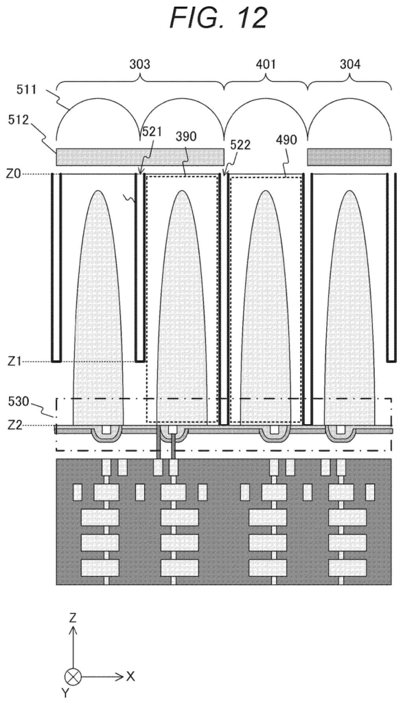
The core claim is that the detection pixel gets a trench isolation (a thin insulating wall cut into the silicon between pixels) in a different pattern than the regular pixel area. The filing describes several versions:

  • A full-depth trench separates the well of the photo pixels from the well of the detection pixel (a well is the doped silicon region where a pixel's circuits sit). This keeps voltage wobble on the shared readout wire from leaking across.
  • The detection pixel's light-to-voltage circuit (log transistors and transimpedance amplifiers, which turn light current into an amplified logarithmic voltage) can use its own power lines, with some wells held at a negative voltage.
  • A shallower rear trench is laid out so it never cuts the detection pixel in two, since variation in a dividing wall made the pixel's behavior vary.
  • Photo pixels next to a detection pixel can be a different size from the rest, to even out their image quality.

The filing also describes stacking transistors in two layers and sharing circuits between two detection pixels, both to make pixels smaller.

Why this matters for robot and car cameras

If you ride in a car with driver-assist cameras or work near factory robots, the camera has to do two things well: record a clean image and notice sudden movement fast. This patent application goes after the second part, because the filing says leakage from the photo pixels lowers how accurately the motion pixels detect changes.

The description names industrial robot cameras and in-vehicle cameras as likely homes, and it ties the chip to a car's outside-view camera that spots pedestrians and obstacles. It also says a depth-measuring pixel could take the place of the motion pixel. No product is named, so treat this as chip-level groundwork that would show up, if at all, as slightly more reliable sensing.

Sony's 36th filing we've tracked since July in the self-driving sensing race builds on one that corrects ranging errors and one on keeping lights even.

Editorial take

The problem here is real, but it is a narrow one. A chip that joins a photo sensor and a motion sensor is only worth building if the motion half stays accurate, and electrical leakage from the photo half chips away at exactly that.

Sony's answer fits the size of the problem. It adds walls, splits some power lines, and adjusts a few pixel sizes, all changes a chip factory could make without redesigning the whole sensor. The filing gives no measured results, so how much cleaner the signal gets is unknown.

You will never see any of this in a photo. Its value would show up as a camera that misses fewer sudden movements, a modest and sensible payoff for a flaw almost nobody notices.

Get our take in your Top Stories

Liked this breakdown? Add Patentlyze as a preferred source on Google, and our plain-English take shows up more often in your Top Stories the next time Sony patent news breaks.

There are more where this came from

We read every patent application Big Tech publishes and send you the ones worth knowing. Plain English, free, every week.

The drawings

68 drawing sheets from US 2026/0352969 A1 · click any drawing to enlarge

Stacking the light sensor directly over its support chip, drawing sheet 1 from US 2026/0352969 A1
Sheet 1 Stacking the light sensor directly over its support chip
Mixing event-sensing pixels directly into regular color pixel grids, drawing sheet 2 from US 2026/0352969 A1
Sheet 2 Mixing event-sensing pixels directly into regular color pixel grids
Supporting circuits that read out and coordinate image signals, drawing sheet 3 from US 2026/0352969 A1
Sheet 3 Supporting circuits that read out and coordinate image signals
Splitting motion-sensing tasks between the upper and lower chip, drawing sheet 4 from US 2026/0352969 A1
Sheet 4 Splitting motion-sensing tasks between the upper and lower chip
Wiring shared color pixels alongside a motion-tracking pixel, drawing sheet 5 from US 2026/0352969 A1
Sheet 5 Wiring shared color pixels alongside a motion-tracking pixel
Connecting standalone pixels directly to their processing circuit, drawing sheet 6 from US 2026/0352969 A1
Sheet 6 Connecting standalone pixels directly to their processing circuit
How motion pixels measure sudden changes in brightness, drawing sheet 7 from US 2026/0352969 A1
Sheet 7 How motion pixels measure sudden changes in brightness
Arranging light sensors and transistors across the top surface, drawing sheet 8 from US 2026/0352969 A1
Sheet 8 Arranging light sensors and transistors across the top surface
Show the other 52 sheets
Grouping motion-sensing transistors together inside a single pixel, drawing sheet 9 from US 2026/0352969 A1
Sheet 9 Grouping motion-sensing transistors together inside a single pixel
Dividing the motion-sensing pixel with internal isolation walls, drawing sheet 10 from US 2026/0352969 A1
Sheet 10 Dividing the motion-sensing pixel with internal isolation walls
Side view showing deep trenches walling off the event pixel, drawing sheet 11 from US 2026/0352969 A1
Sheet 11 Side view showing deep trenches walling off the event pixel
Another cross section showing how deep trenches isolate adjacent pixels, drawing sheet 12 from US 2026/0352969 A1
Sheet 12 Another cross section showing how deep trenches isolate adjacent pixels
Deep barrier walls stopping electric charge from leaking sideways, drawing sheet 13 from US 2026/0352969 A1
Sheet 13 Deep barrier walls stopping electric charge from leaking sideways
Shallow barriers that let electrical noise spill into neighbors, drawing sheet 14 from US 2026/0352969 A1
Sheet 14 Shallow barriers that let electrical noise spill into neighbors
Power lines across the sensor grid keep voltage steady, drawing sheet 15 from US 2026/0352969 A1
Sheet 15 Power lines across the sensor grid keep voltage steady
Wiring that splits pixel controls across two stacked sensor chips, drawing sheet 16 from US 2026/0352969 A1
Sheet 16 Wiring that splits pixel controls across two stacked sensor chips
Encasing only one event-sensing pixel inside an insulating trench wall, drawing sheet 17 from US 2026/0352969 A1
Sheet 17 Encasing only one event-sensing pixel inside an insulating trench wall
Isolating specific converter circuits inside their own trench perimeter, drawing sheet 18 from US 2026/0352969 A1
Sheet 18 Isolating specific converter circuits inside their own trench perimeter
Walling off high-speed amplifier components across different pixel rows, drawing sheet 19 from US 2026/0352969 A1
Sheet 19 Walling off high-speed amplifier components across different pixel rows
Staggering isolated sensor circuits across adjacent pixel spaces, drawing sheet 20 from US 2026/0352969 A1
Sheet 20 Staggering isolated sensor circuits across adjacent pixel spaces
Surrounding regular color pixels and event sensors with isolation walls, drawing sheet 21 from US 2026/0352969 A1
Sheet 21 Surrounding regular color pixels and event sensors with isolation walls
Subdividing the pixel grid to maintain uniform isolation wall patterns, drawing sheet 22 from US 2026/0352969 A1
Sheet 22 Subdividing the pixel grid to maintain uniform isolation wall patterns
Stacking pixel circuits across two chips to save space, drawing sheet 23 from US 2026/0352969 A1
Sheet 23 Stacking pixel circuits across two chips to save space
Splitting sensor electronics across upper and lower silicon tiers, drawing sheet 24 from US 2026/0352969 A1
Sheet 24 Splitting sensor electronics across upper and lower silicon tiers
Spreading motion-sensing parts across upper and lower chip layers, drawing sheet 25 from US 2026/0352969 A1
Sheet 25 Spreading motion-sensing parts across upper and lower chip layers
A circuit using one switch to track brightness changes, drawing sheet 26 from US 2026/0352969 A1
Sheet 26 A circuit using one switch to track brightness changes
Adding a second logarithmic switch to boost light detection sensitivity, drawing sheet 27 from US 2026/0352969 A1
Sheet 27 Adding a second logarithmic switch to boost light detection sensitivity
Stacking three logarithmic switches across the two sensor chips, drawing sheet 28 from US 2026/0352969 A1
Sheet 28 Stacking three logarithmic switches across the two sensor chips
Powering motion and picture pixels through separate wires, drawing sheet 29 from US 2026/0352969 A1
Sheet 29 Powering motion and picture pixels through separate wires
Routing separate power lines horizontally across the pixel grid, drawing sheet 30 from US 2026/0352969 A1
Sheet 30 Routing separate power lines horizontally across the pixel grid
Powering motion detection circuits with an independent negative voltage, drawing sheet 31 from US 2026/0352969 A1
Sheet 31 Powering motion detection circuits with an independent negative voltage
Electrical model showing how negative supply wires cut pixel interference, drawing sheet 32 from US 2026/0352969 A1
Sheet 32 Electrical model showing how negative supply wires cut pixel interference
Adjusting electrical bias drains signal charge more completely, drawing sheet 33 from US 2026/0352969 A1
Sheet 33 Adjusting electrical bias drains signal charge more completely
Routing dedicated voltage lines across motion and color pixels, drawing sheet 34 from US 2026/0352969 A1
Sheet 34 Routing dedicated voltage lines across motion and color pixels
Sharing conversion parts across vertically separated motion pixels, drawing sheet 35 from US 2026/0352969 A1
Sheet 35 Sharing conversion parts across vertically separated motion pixels
Running two separate power lines across staggered motion pixels, drawing sheet 36 from US 2026/0352969 A1
Sheet 36 Running two separate power lines across staggered motion pixels
Combining signals between neighboring motion sensor pixels, drawing sheet 37 from US 2026/0352969 A1
Sheet 37 Combining signals between neighboring motion sensor pixels
Insulating trench walls surrounding motion and color pixel zones, drawing sheet 38 from US 2026/0352969 A1
Sheet 38 Insulating trench walls surrounding motion and color pixel zones
Stretching a motion pixel to cover two unit cell spaces, drawing sheet 39 from US 2026/0352969 A1
Sheet 39 Stretching a motion pixel to cover two unit cell spaces
Expanding motion sensing pixels across three unit areas, drawing sheet 40 from US 2026/0352969 A1
Sheet 40 Expanding motion sensing pixels across three unit areas
Shaping a motion sensor around color pixels, drawing sheet 41 from US 2026/0352969 A1
Sheet 41 Shaping a motion sensor around color pixels
T-shaped motion sensor nested neatly among standard color pixels, drawing sheet 42 from US 2026/0352969 A1
Sheet 42 T-shaped motion sensor nested neatly among standard color pixels
Corner layout spreading a motion sensor across pixels, drawing sheet 43 from US 2026/0352969 A1
Sheet 43 Corner layout spreading a motion sensor across pixels
Stepped sensor boundaries shielding motion detectors from neighboring cells, drawing sheet 44 from US 2026/0352969 A1
Sheet 44 Stepped sensor boundaries shielding motion detectors from neighboring cells
Placing a tall sensor between pixel columns, drawing sheet 45 from US 2026/0352969 A1
Sheet 45 Placing a tall sensor between pixel columns
Traditional trench walls running between every single subpixel, drawing sheet 46 from US 2026/0352969 A1
Sheet 46 Traditional trench walls running between every single subpixel
Inside wall separating pixels from an empty cavity, drawing sheet 47 from US 2026/0352969 A1
Sheet 47 Inside wall separating pixels from an empty cavity
Comparing full barrier grids with one continuous motion-detecting pixel, drawing sheet 48 from US 2026/0352969 A1
Sheet 48 Comparing full barrier grids with one continuous motion-detecting pixel
Removing an internal barrier creates one large light sensor, drawing sheet 49 from US 2026/0352969 A1
Sheet 49 Removing an internal barrier creates one large light sensor
Spacing motion-sensing pixels across a row of color pixels, drawing sheet 50 from US 2026/0352969 A1
Sheet 50 Spacing motion-sensing pixels across a row of color pixels
Placing motion pixels diagonally two columns and one row apart, drawing sheet 51 from US 2026/0352969 A1
Sheet 51 Placing motion pixels diagonally two columns and one row apart
Shifting motion pixels diagonally into neighboring rows and columns, drawing sheet 52 from US 2026/0352969 A1
Sheet 52 Shifting motion pixels diagonally into neighboring rows and columns
Aligning motion-sensing pixels vertically in the same column, drawing sheet 53 from US 2026/0352969 A1
Sheet 53 Aligning motion-sensing pixels vertically in the same column
Positioning motion pixels diagonally across two full rows, drawing sheet 54 from US 2026/0352969 A1
Sheet 54 Positioning motion pixels diagonally across two full rows
Arranging motion pixels diagonally at the opposite chip corner, drawing sheet 55 from US 2026/0352969 A1
Sheet 55 Arranging motion pixels diagonally at the opposite chip corner
Pairing two motion-sensing pixels side by side horizontally, drawing sheet 56 from US 2026/0352969 A1
Sheet 56 Pairing two motion-sensing pixels side by side horizontally
Stacking motion sensing pixels vertically between color pixels, drawing sheet 57 from US 2026/0352969 A1
Sheet 57 Stacking motion sensing pixels vertically between color pixels
Shrinking the motion pixel leaves extra space for standard pixels, drawing sheet 58 from US 2026/0352969 A1
Sheet 58 Shrinking the motion pixel leaves extra space for standard pixels
Expanding the motion pixel sideways and vertically for better sensitivity, drawing sheet 59 from US 2026/0352969 A1
Sheet 59 Expanding the motion pixel sideways and vertically for better sensitivity
Slimming motion pixels to fit crowded sensors, drawing sheet 60 from US 2026/0352969 A1
Sheet 60 Slimming motion pixels to fit crowded sensors

Sheets 61 to 68 are in the full USPTO filing.

Browse all the drawings 68 drawing sheets
Patent filing page

Source. Full patent text and figures from the official USPTO publication PDF.
Reader comments

Be the first to weigh in

Start the discussion

Real name or a handle, either is fine. Comments are read by a person before they appear, so allow a little time. Keep it about the filing.