Sony Patents a Way to Stop Camera Pixels from Interfering with Each Other
Every time a digital camera converts light into data, it creates electrical noise that can corrupt nearby pixels. Sony's new patent describes a way to keep two different types of pixels from interfering with each other on the same sensor chip.
How Sony's sensor keeps two pixel jobs from clashing
Imagine your camera sensor as a busy office where two teams share the same electrical wiring. One team is constantly digitizing data — converting raw light measurements into numbers your phone or camera can store. That process isn't quiet: it causes tiny voltage spikes on the shared wiring, which can disturb the other team trying to detect sudden changes in the scene.
Sony's patent proposes a fix: give the second team — the pixels that watch for sudden events, like a flash of light or a fast-moving object — their own holding circuit that actively cancels out the noise caused by the first team's digitizing work. It essentially puts up a buffer so the two jobs don't step on each other.
This matters most in event-based sensors, a type of image sensor that flags changes in a scene rather than snapping full frames. These sensors are increasingly used in robotics, drones, and high-speed cameras where split-second detection matters.
How the signal-holding circuit isolates event pixels from ADC noise
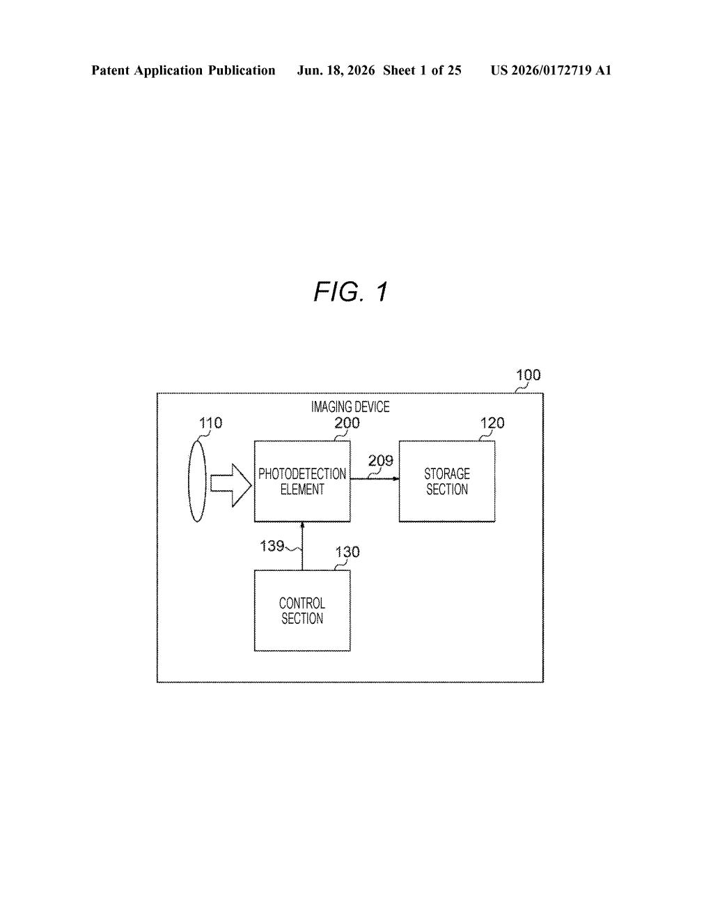
The patent describes a photodetection element (basically a chip with an array of light-sensing pixels) that handles two different kinds of pixels simultaneously on the same surface.
- First pixels feed their output through a signal line into a conversion section — an analog-to-digital converter (ADC) that turns raw voltage readings from light into binary numbers a processor can use.
- Second pixels are responsible for event detection: they watch for moments when their output crosses a set threshold, which indicates something in the scene changed suddenly.
- A signal holding section sits between the second pixels and the detection circuit. During the periods when the ADC is actively converting data, this holding section clamps or stabilizes the second pixel's output so that the electrical noise generated by the ADC — which travels along shared wiring — doesn't cause false event triggers.
The key insight is timing: ADC conversion happens in cycles, and the noise it produces is predictable. The holding circuit uses that timing information to know exactly when to suppress fluctuations. The result is a sensor where frame-based imaging and event-based detection can coexist on the same chip without one corrupting the other.
What this means for Sony's camera and sensor business
Event-based image sensors are a growing area for Sony, which supplies sensors to smartphone makers, robotics companies, and automotive camera systems. The core problem this patent solves — ADC noise bleeding into event-detection circuits — is a real engineering headache when you try to combine both functions on one chip. Solving it cleanly could make hybrid sensors (ones that do both traditional imaging and event detection) more practical and cheaper to build.
For you as a consumer, this kind of work shows up eventually in things like faster autofocus, more reliable motion detection in security cameras, or better low-light performance in phones. It's not a feature you'd see advertised on a spec sheet, but it's the kind of foundational chip design that determines whether a sensor can be pushed further.
This is tightly scoped semiconductor engineering — not the kind of patent that signals a product launch, but exactly the kind that determines whether a company can build hybrid event sensors that actually work reliably. Sony's sensor division is one of the most important in the world, and patents like this reflect real design problems they're actively solving. Worth a note, but not worth breathless coverage.
Get one Big Tech patent every Sunday
Plain English, intelligent commentary, no hype. Free.
Editorial commentary on a publicly published patent application. Not legal advice.