Samsung Patents a Single-Substrate Growth Method for Full-Color Micro LED Displays
One of the biggest manufacturing headaches in micro LED display tech is growing red, green, and blue pixels separately and then assembling them. Samsung's new patent describes a way to grow all three colors on the same substrate — which could be a meaningful step toward making micro LED displays practical at scale.
What Samsung's single-substrate micro LED trick actually does
Imagine trying to assemble a tiny mosaic where every single tile is a different color and has to come from a different factory. That's roughly the problem with building micro LED displays today — red, green, and blue pixels are typically grown separately and then painstakingly combined. It's expensive, slow, and hard to scale down to high resolutions.
Samsung's patent describes a fabrication method that grows all three colors of light-emitting structures on the same substrate, one color at a time, using a process called selective area growth. Think of it like building up each color's tiny LED tower in sequence, using carefully patterned insulating layers to control exactly where each one grows.
Once all three colors are built together, the entire pixel array can be transferred to a display backplane in a single step rather than three separate transfers. That single-transfer approach is the practical payoff — fewer steps means fewer chances for misalignment and lower manufacturing costs.
How selective area growth builds each color LED in sequence
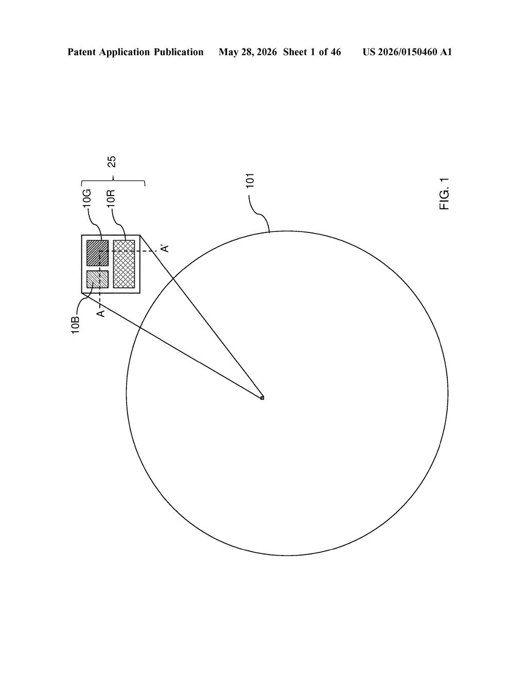
The patent describes a multi-step lithographic fabrication sequence for building multicolor micro LED pixel arrays where red, green, and blue subpixels are all grown on the same initial substrate.
The core technique is selective area growth (SAG) — a process where a dielectric (insulating) mask layer is patterned with tiny openings, and semiconductor material grows only within those openings rather than everywhere. This gives precise spatial control over where each LED structure forms. The process repeats for each color:
- A dielectric mask layer is deposited and lithographically patterned (meaning UV light and chemicals are used to etch a precise pattern into it).
- A small semiconductor pedestal structure grows up through the opening — essentially a seed post for the LED.
- The full LED stack — including the active region (the quantum-well layer that actually emits light) and the top semiconductor layer — grows upward from that pedestal.
- The mask is etched away, a new mask is deposited, and the sequence repeats for the next color wavelength.
Because each color's active region is tuned to emit at a different peak wavelength (blue, green, and red), the result is a complete RGB subpixel set sitting side by side on one substrate. The entire array is then transferred to a display backplane (the electronics layer that drives each pixel) in a single mass-transfer step — a significant simplification over transferring three separate color arrays.
What this means for the future of micro LED display costs
Micro LED is widely seen as the display technology that could eventually replace OLED — it's brighter, more power-efficient, and potentially longer-lasting. But the manufacturing complexity has kept it confined to very expensive, large-format displays. The ability to grow all three colors monolithically on one substrate and transfer them in one shot directly attacks the two biggest cost drivers: yield loss during multi-transfer assembly and the complexity of aligning sub-micron pixels across separate color wafers.
For you as a consumer, this kind of process innovation is what would eventually make micro LED viable in a phone or a smartwatch rather than just a $100,000 TV. Samsung is one of the few companies with both the display manufacturing scale and the semiconductor fabrication expertise to actually commercialize something like this — so this filing is worth tracking.
This is a genuinely substantive patent, not a defensive placeholder. Monolithic multicolor micro LED fabrication is one of the field's hardest open problems, and Samsung's selective-area-growth approach with sequential dielectric masking is a real engineering proposal with a clear path to reducing transfer complexity. Whether it yields better results than competing approaches — like color conversion using quantum dots — is an open question, but the patent shows Samsung is working on the problem at the process level, not just the system level.
Get one Big Tech patent every Sunday
Plain English, intelligent commentary, no hype. Free.
Editorial commentary on a publicly published patent application. Not legal advice.