OpenAI Patents a Tiled Chip Architecture That Does AI Math Inside Memory
OpenAI is designing its own chip architecture — and it's built around a simple but powerful idea: do the math where the data lives, not somewhere else.
What OpenAI's in-memory compute tiles actually do
Here's a quick analogy: imagine your calculator had to drive across town to fetch every number before it could add them up. That's roughly what traditional chips do — they shuttle data from memory to a processor, crunch it, then send results back. It's fast, but all that travel adds up in time and power.
OpenAI's patent describes a different approach. Instead of moving data to the processor, the processor comes to the data. Small, self-contained units called compute tiles store the numbers (called weights) they need and do the multiplication right there in memory. A lightweight general-purpose processor sits alongside each tile to handle the trickier math — like the nonlinear functions neural networks need — and to keep things coordinated.
The tiles are designed to talk to each other too, with a built-in conversion engine that translates data between tiles when their formats don't match. Think of it like an automatic language translator sitting on the data highway between chips.
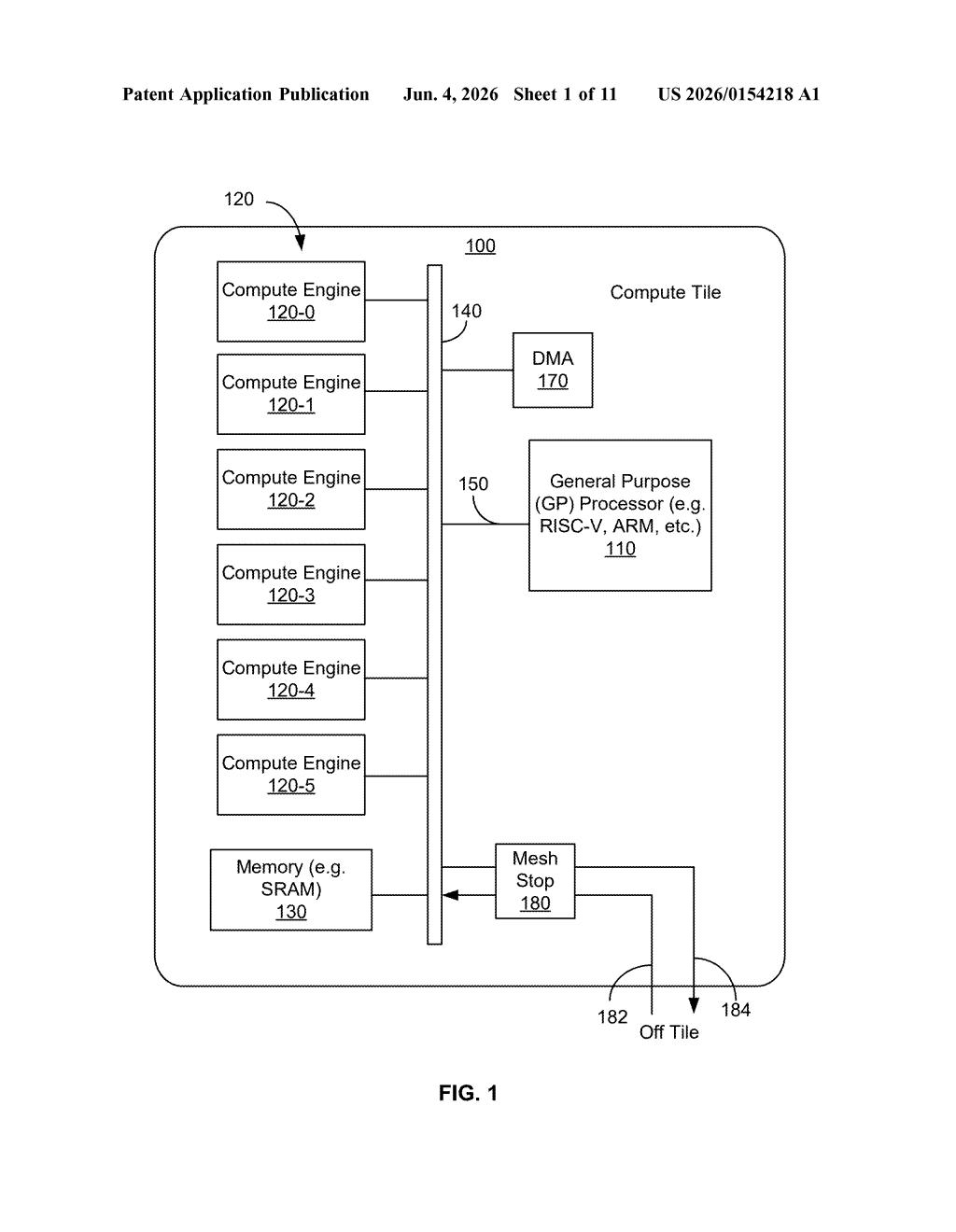
How the CIM tiles, GP processor, and data conversion fit together
The patent describes a tiled compute architecture where each tile is a self-contained AI processing unit. Here's how the pieces fit together:
- Compute-in-memory (CIM) modules — each engine stores a matrix of neural network weights and performs vector-matrix multiplication (VMM) (the core math operation in AI inference — multiplying an input vector against a weight matrix) directly inside the memory hardware, skipping the usual fetch-and-compute cycle.
- General-purpose (GP) processor per tile — sits alongside the CIM engines, handles nonlinear operations like activation functions (e.g., ReLU, sigmoid), and orchestrates the engines. Crucially, data can move around the GP processor via bypass paths, so it doesn't become a bottleneck.
- Addressable compute engines — external data movement initiators can push or pull data directly to/from engines without going through the GP processor, enabling parallel, low-latency data transfers.
- Data conversion engine — when one tile outputs data in one numeric format and the next tile expects a different one, this converter handles the translation on the fly, letting tiles with different precision or data types work together in a single pipeline.
The multi-tile design means you can chain or array these tiles to scale up compute for larger models.
What this means for the future of AI accelerator chips
The biggest bottleneck in running large AI models isn't the math — it's moving data. Memory bandwidth is expensive in both time and power, and compute-in-memory architectures are one of the most promising ways to close that gap. If OpenAI is patenting this kind of hardware, it signals they're thinking seriously about building custom silicon optimized for their own inference workloads, not just renting GPU time from Nvidia.
For you as a user, the downstream effect would be AI responses that are faster and cheaper to generate — which matters a lot when OpenAI is serving hundreds of millions of queries. The inter-tile data conversion engine is a particularly practical touch: it means you can mix precision levels across a chip, trading off accuracy for speed in layers where it won't hurt quality.
This is a genuinely substantive hardware patent, not a paper exercise. The specific combination of CIM engines, per-tile GP processors, bypass data paths, and a format-conversion bridge between tiles reads like a real chip microarchitecture spec, not a vague concept filing. OpenAI patenting this kind of low-level silicon work is the clearest signal yet that they're serious about owning their own compute stack end-to-end.
Get one Big Tech patent every Sunday
Plain English, intelligent commentary, no hype. Free.
Editorial commentary on a publicly published patent application. Not legal advice.