Samsung Patents Semiconductor Package With Embedded Chip Capacitors in Substrate
Samsung is filing patents on a packaging technique that buries capacitors inside the circuit substrate itself — not on top of it — which could mean cleaner power delivery and smaller chip footprints for high-end processors.
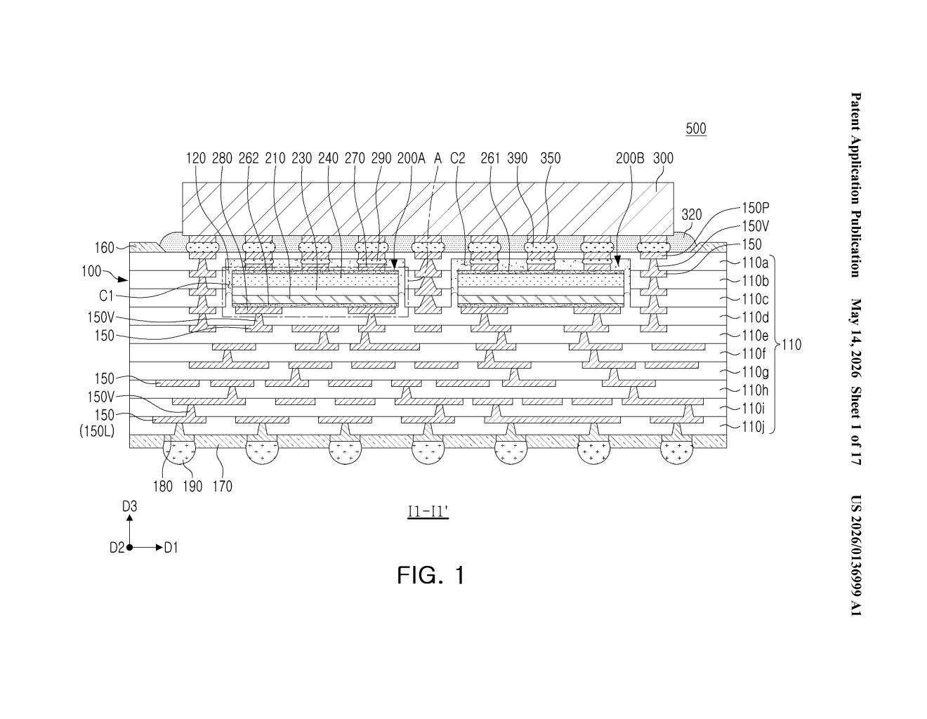
What Samsung's embedded capacitor substrate actually does
Imagine your smartphone's processor is like a high-performance engine. Engines need a steady fuel supply, and chips need a steady power supply. Tiny components called capacitors act like small power reservoirs, smoothing out voltage spikes before they can scramble your chip's calculations. Normally, these capacitors sit on top of or around the chip — taking up valuable space and adding distance to the power path.
Samsung's patent describes a smarter arrangement: hollow pockets (cavities) are carved directly into the layers of the substrate — the circuit board the chip sits on — and semiconductor-based capacitors are slotted right inside those cavities. The capacitors connect to the surrounding wiring above and below them, putting power reserves much closer to where the chip actually needs them.
The result is a more compact package where power doesn't have to travel as far, which is especially valuable in dense, high-speed chips where even tiny electrical delays matter.
How the cavities and dual-pad wiring connections work
The patent describes a coreless circuit substrate — a substrate that skips the traditional rigid core layer in favor of multiple stacked insulating layers, which allows it to be thinner and to have cavities machined into it. Those cavities are precisely where this invention gets interesting.
Semiconductor-based chip capacitors (capacitors made from silicon or similar semiconductor material, as opposed to older ceramic types) are placed into those cavities. Each capacitor has:
- First pads on its top surface, connected upward to an adjacent wiring layer via conductive bumps (tiny solder or copper bumps, similar to flip-chip interconnects)
- Second pads on its bottom surface, connected downward directly into the interconnection vias (vertical copper pathways that link wiring layers) of the layer below
This dual-sided connection means the capacitor is fully integrated into the substrate's wiring stack — not just passively sitting in a hole, but actively wired into the signal and power distribution network above and below it.
The main semiconductor chip sits on top of the whole assembly, connected to the uppermost wiring layer. From the chip's perspective, power-smoothing capacitance is immediately beneath it, embedded in the substrate itself rather than mounted separately.
What this means for high-performance chip packaging
For high-performance chips — think data center CPUs, AI accelerators, or advanced mobile SoCs — power integrity is a serious engineering challenge. The closer your decoupling capacitors are to the chip, the less inductance (electrical resistance to rapid current changes) you fight, and the more stable your voltage rail stays under heavy computation loads. Embedding capacitors inside the substrate rather than attaching them to the surface cuts that distance dramatically.
This also has a form-factor benefit: fewer components on the package surface means more room for other circuitry or a smaller overall footprint. As Samsung competes with TSMC and Intel Foundry on advanced packaging for AI and HPC customers, techniques like this are part of a larger race to differentiate at the packaging level — not just at the silicon node.
This is a competent, well-scoped packaging patent — not flashy, but squarely aimed at a real engineering problem. Embedded decoupling capacitors are a legitimate area of active development across the industry, and Samsung filing on a specific coreless-substrate implementation shows they're investing seriously in advanced packaging infrastructure. Worth tracking if you follow semiconductor packaging competition.
Get one Big Tech patent every Sunday
Plain English, intelligent commentary, no hype. Free.
Editorial commentary on a publicly published patent application. Not legal advice.