
Samsung Patents a Wrapped FPCB Battery Connection for Foldable Phones
Getting a battery and a motherboard to talk to each other sounds trivial — until you're doing it inside a foldable phone where every fraction of a millimeter counts. Samsung's latest patent is all about a smarter way to route that connection.
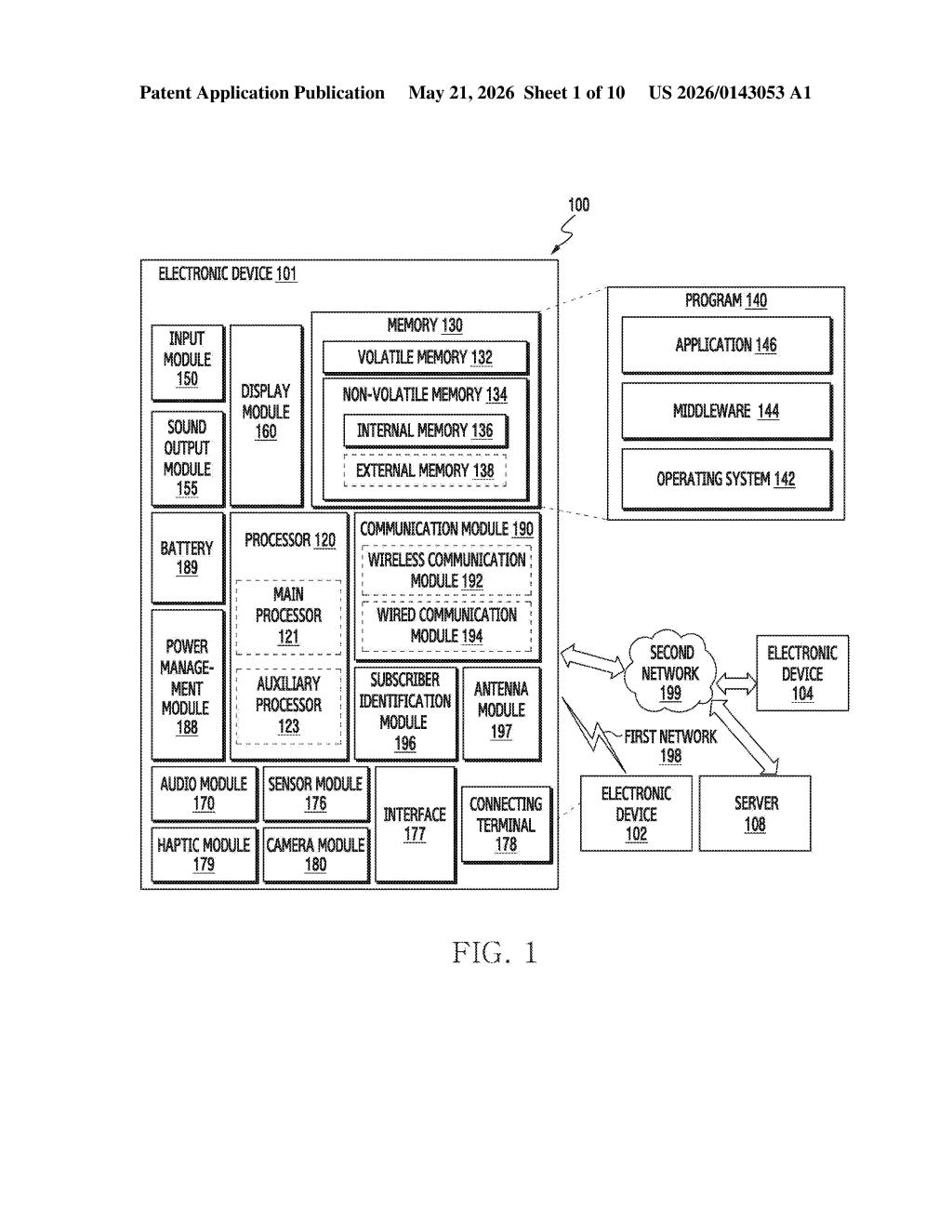
What Samsung's battery ribbon routing actually does
Imagine trying to wire up two components inside a book that folds in half — and the wire has to go around the spine without bunching up or breaking. That's roughly the problem Samsung is solving here.
Inside a foldable phone, the battery and the main circuit board sit on opposite sides of each other. A thin, flexible ribbon cable (called an FPCB) has to connect them. The obvious approach — running the cable over the top or under the bottom — wastes precious space or creates stress points that can crack over time.
Samsung's design routes that ribbon cable around the side edge of the circuit board instead. One end connects to the battery below the board, the cable wraps around the board's side surface, and the other end connects to the front face of the board. It's a neater path that keeps the internals compact and the connection stable across thousands of folds.
How the FPCB bends around the PCB's side edge
The patent describes a flexible printed circuit board (FPCB) — a thin, bendable ribbon cable — used to connect the battery to the main PCB inside the second (larger) housing of a foldable device.
The FPCB is divided into three functional portions:
- First portion: connects to the battery and sits on the back side of the PCB (the side facing away from the display)
- Second portion: connects to the front face of the PCB (the side facing the display)
- Third portion: the routing segment that travels from the first portion, around the side edge of the PCB, to reach the second portion
The key detail is that the third portion includes a section bent around the side surface of the PCB — the thin edge between its front and back faces. This means the cable doesn't have to loop around the top or bottom of the board, which would require more slack, more space, or both.
The design is framed around the constraints of the second housing specifically, which contains the display, battery, and PCB in a tightly stacked arrangement — the kind of dense layering that foldable form factors demand.
What this means for thinner, denser foldable designs
Foldable phones are essentially an engineering war against thickness and fragility. Every internal routing decision affects how thin the device can be, how reliably it survives repeated folding, and how much room remains for a larger battery. A cable path that wraps cleanly around a board edge instead of looping over or under it is a small win — but in foldable design, small wins add up fast.
For Samsung's Galaxy Z Fold and Z Flip lines, iterating on internal component routing is a steady part of each generation's engineering work. This patent suggests the team is actively rethinking how power connections are laid out — which could contribute to marginally slimmer builds or more flexible internal layouts in future devices.
This is unglamorous but real engineering work — the kind of incremental internal geometry improvement that separates good foldable hardware from great foldable hardware. It won't headline a product launch, but patents like this are exactly how Samsung chips away at the thickness and durability tradeoffs that still hold foldables back.
Get our take in your Top Stories
Liked this breakdown? Add Patentlyze as a preferred source on Google, and our plain-English take shows up more often in your Top Stories the next time Samsung patent news breaks.
There are more where this came from
We read every patent application Big Tech publishes and send you the ones worth knowing. Plain English, free, every week.
Want this weekly breakdown for a company we don't cover? Patentlyze Pro →