
Google Patents a Two-Track Noise-Cancellation Chip That Saves Battery
Google is rethinking how noise-cancellation chips work, splitting the job across two parallel processing tracks so your headphones can react fast to sudden noise while still preserving battery life.
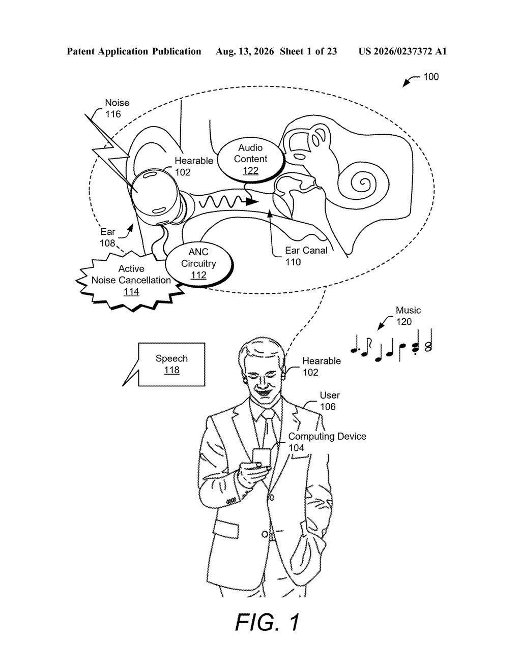
What Google's two-path ANC chip actually does
You're on a long flight with noise-canceling headphones and the engine roar suddenly shifts pitch. Your headphones need to react almost instantly or you'll hear a burst of noise. But reacting fast costs battery, and doing it constantly drains your headphones in hours instead of days.
Google's new patent tries to solve that by giving the noise-cancellation chip two separate lanes. One lane runs fast, catching sudden changes in real time. The other runs slow, handling slower, more predictable background noise without burning through power. A third, middle-speed lane fills in the gap between them.
The result, at least in theory, is headphones that feel responsive when they need to be and power-efficient the rest of the time. It's the same idea as a car that shifts between driving modes automatically, except it's happening inside a chip you can't see, thousands of times per second.
… generating, using the active-noise-cancellation circuitry, at least one second anti-noise signal component by processing the input noise reference signal in accordance with a pulse-code-modulation domain and using at least one second processing rate, the at least one second processing rate being slower than the at least one first processing rate …
Translation: The chip creates a second anti-noise signal more slowly to save energy.
How the fast and slow processing paths split the work
The patent describes active noise cancellation (ANC) circuitry that runs three parallel processing paths simultaneously, each operating at a different speed and using a different signal format.
The first path uses a signal format called pulse-density modulation (PDM), which represents audio as a very rapid stream of single-bit pulses. PDM is well-suited to high-speed processing, so this path runs fast enough to catch sudden, sharp changes in ambient noise. The patent specifically notes that PDM's structure makes it easier to build low-power tunable filters in this path.
The second path uses pulse-code modulation (PCM), the standard digital audio format used in most consumer electronics (think CD-quality audio). PCM runs at a much slower rate here. The tradeoff is speed for flexibility: PCM's format gives engineers more room to design complex, finely tuned filters that handle steady background noise. A third path runs at a middle speed and can use either format, bridging the gap.
All three paths generate their own partial anti-noise signal (an inverted copy of incoming noise), and the chip combines these three components into one final anti-noise output. The goal is a signal that is both fast-reacting and frequency-accurate without requiring a single power-hungry processor to do everything at once.
The pulse-density-modulation domain enables a tunable filter within the at least one first processing path to be designed in a manner that reduces power consumption.
Translation: One specific signal format helps the filter design use less power.
What this means for the next Pixel Buds
If this approach makes it into consumer hardware, the practical payoff is ANC headphones that handle two problems that currently trade off against each other: reaction speed for sudden noise events and battery life during long listening sessions. Existing ANC chips typically run one unified processing path and tune it as a compromise between speed and efficiency. Splitting the work across dedicated paths could let engineers optimize each one independently.
For Google, this sits squarely in the hardware stack behind the Pixel Buds line and any future Tensor-based audio chips. The audio chip design space is one of the more technically contested areas in the latest Big Tech patents, with Apple, Samsung, and Qualcomm all filing aggressively around ANC efficiency. Whether Google's multi-path approach ever ships is a separate question, but the engineering logic here is coherent.
The design bets that splitting one unified noise-cancellation path into three specialized ones is worth the added circuit complexity. That's a real cost: more silicon area, more potential failure modes, and more engineering effort to synchronize three paths so they don't cancel each other out or introduce phase artifacts. The PDM-for-speed, PCM-for-flexibility split is technically sensible, but the actual power savings depend entirely on how aggressively the slow PCM path can idle. If the middle-speed path has to run continuously rather than selectively, the efficiency gains shrink considerably. The trade reads as worth pursuing for premium ANC hardware where battery life is a genuine differentiator, though it's an open question whether the complexity pays off in a $99 earbud.
There are more where this came from
We read every patent application Big Tech publishes and send you the ones worth knowing. Plain English, free, every week.
The drawings
23 drawing sheets from US 2026/0237372 A1 · click any drawing to enlarge


Want this weekly breakdown for a company we don't cover? Patentlyze Pro →
Be the first to weigh in