Samsung Patents a Chip That Shares Overlapping Image Edge Data to Accelerate Processing
When a chip processes an image in chunks, the edges of each chunk are a headache — every chunk needs to peek at its neighbor to get the math right. Samsung's new patent tackles that problem head-on by pre-copying those border pixels before any computation begins.
What Samsung's image-tile border-copying actually does
Imagine you're assembling a jigsaw puzzle, but your rule is that you can only look at one piece at a time. The problem: figuring out how a piece fits requires seeing the pieces around it. AI chips face exactly this issue when they process images in small rectangular sections called tiles — each tile needs a little information from the tiles next to it to avoid visible seams or calculation errors.
Samsung's patent describes a system that, before any heavy computation starts, takes each tile and quietly copies the relevant border pixels from its neighbors onto the tile itself. So when the chip actually starts crunching numbers, every tile is already self-contained — no need to stop mid-calculation and go fetch data from somewhere else in memory.
The result is smoother, faster image processing because the chip spends less time waiting around for data. This kind of approach is especially useful in neural network workloads — the AI calculations that power features like photo enhancement, object detection, and video upscaling.
How the chip duplicates pixels across adjacent tiles
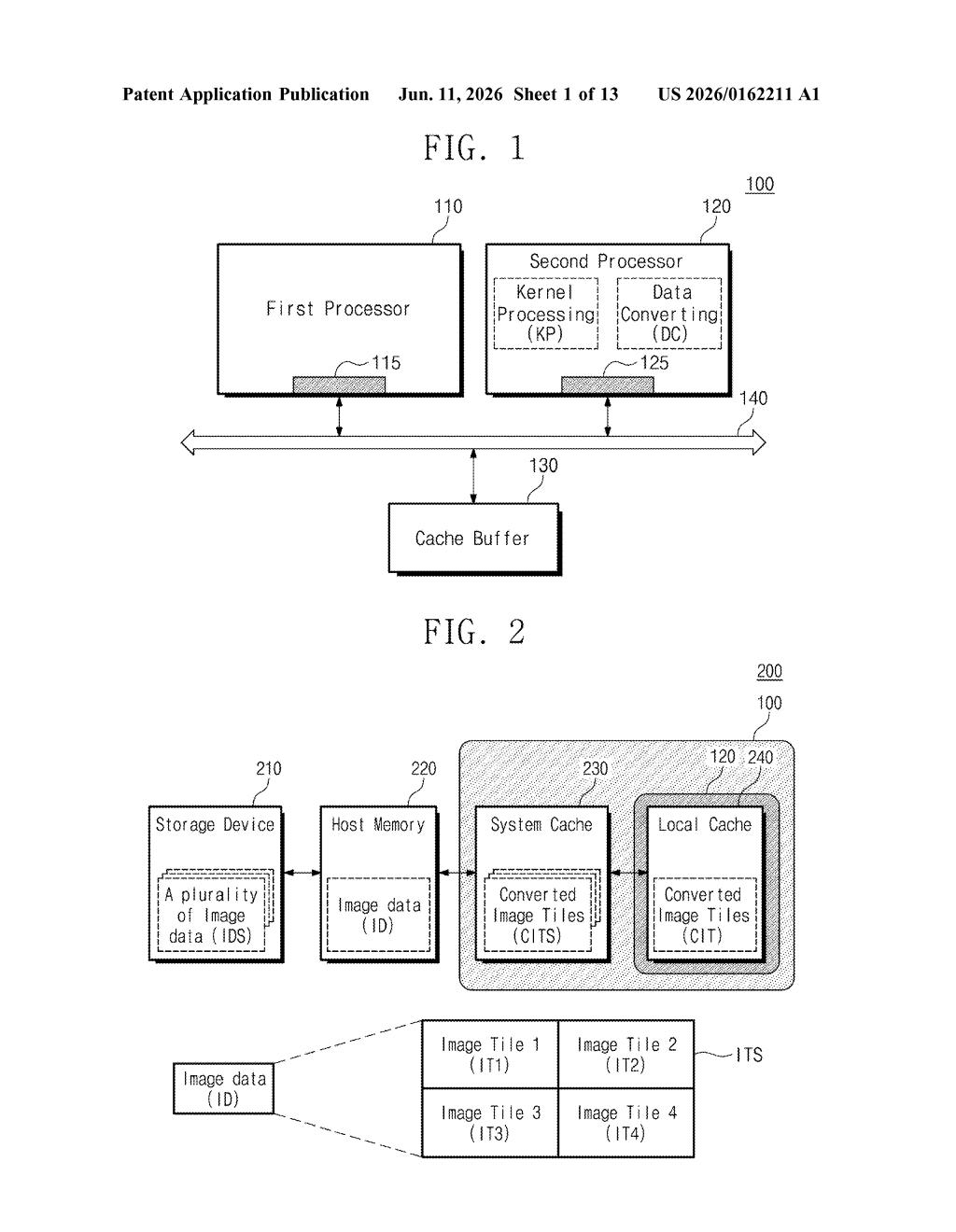
The patent describes a method for a system-on-chip (SoC) — the all-in-one processor found in phones, tablets, and AI accelerators — to handle image data more efficiently by restructuring how image tiles are prepared for computation.
When an image is divided into tiles for parallel processing, many common AI operations (called convolution kernels — think of them as small filters slid across the image to detect edges, textures, or objects) need pixel data from outside their assigned tile's boundaries. Traditionally, that means repeated memory fetches during processing, which introduces delays.
Samsung's approach creates "converted" tiles: an expanded version of each original tile that already includes the necessary border pixels copied from adjacent tiles. Specifically:
- The first converted tile contains all pixels from tile one, plus the relevant edge pixels from tile two.
- The second converted tile contains all pixels from tile two, plus the relevant edge pixels from tile one.
- Both converted tiles are stored across a memory hierarchy (local cache → system cache → host memory → storage) before kernel processing begins.
This means each processing unit gets everything it needs upfront, reducing mid-computation memory traffic and improving throughput on neural network inference tasks.
What this means for AI image processing on Samsung chips
For Samsung, this matters most in its Exynos SoC lineup and AI accelerator products, where on-device neural network inference (photo processing, video enhancement, real-time object detection) is increasingly a selling point. Reducing memory stalls during convolution operations translates directly into faster processing and lower power consumption — both critical in mobile chips where battery life is non-negotiable.
For you as an end user, the downstream effect could show up as faster photo editing, smoother real-time camera filters, or snappier AI-powered video features. It's the kind of low-level plumbing improvement that rarely gets a product slide but quietly makes everything feel faster.
This is unglamorous but solid chip engineering — the kind of data-movement optimization that separates fast AI chips from great ones. Samsung is clearly thinking carefully about memory bandwidth bottlenecks in its neural processing pipelines, and a pre-copy approach like this is a well-established strategy. It won't headline a keynote, but it's the sort of work that shows up in benchmark wins.
Get one Big Tech patent every Sunday
Plain English, intelligent commentary, no hype. Free.
Editorial commentary on a publicly published patent application. Not legal advice.