Samsung Patents a Symmetrical Magnetic Field Design for Chip Coating Equipment
Chip manufacturing lives or dies on coating uniformity — and Samsung's latest patent targets a surprisingly overlooked weak point: the magnetic field that controls the plasma during thin-film deposition.
What Samsung's PVD magnetic field tweak actually does
Imagine spray-painting a surface, but the spray nozzle has a slightly uneven pressure on one side. The result is a coating that's thicker in some spots and thinner in others. At the nanometer scales used in semiconductor manufacturing, that kind of unevenness can ruin a chip entirely.
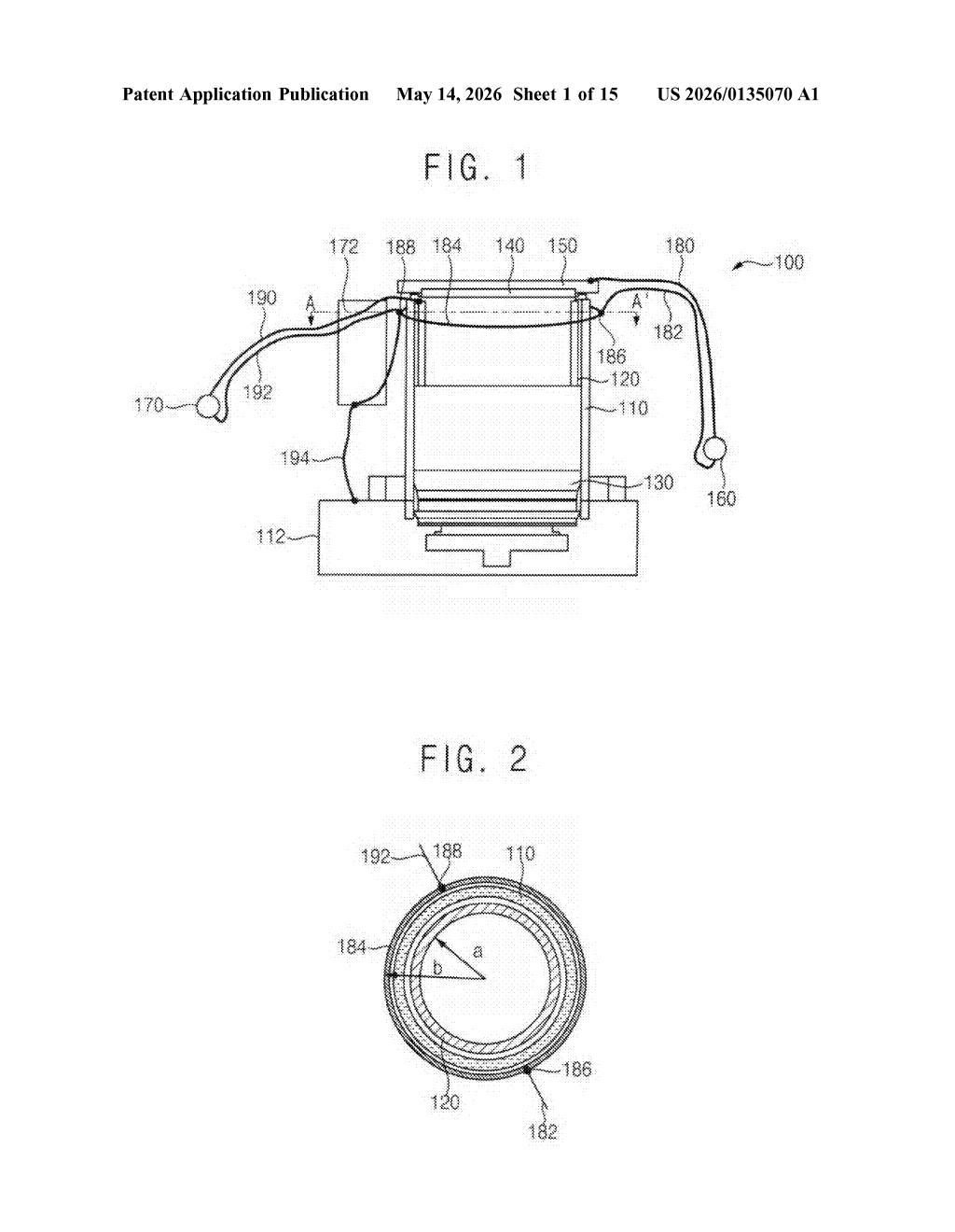
Samsung's patent describes a redesigned piece of equipment called a physical vapor deposition (PVD) apparatus — a machine that coats silicon wafers with ultra-thin films of metal or other materials during chip fabrication. The key innovation is a magnetic field formation line (essentially a wire loop) that wraps symmetrically around the inside of the chamber. By connecting both ends of this loop in a balanced, mirror-image arrangement, Samsung aims to produce a more uniform magnetic field — and, in turn, a more even plasma distribution.
More even plasma means more consistent coatings across the wafer. That's a big deal when you're trying to manufacture billions of identical transistors.
How the symmetric coil loop controls plasma in the chamber
A PVD machine works by bombarding a target (a chunk of the material you want to deposit, like titanium or tungsten) with plasma — an ionized gas — so that atoms fly off and settle onto the substrate (your silicon wafer). A magnet near the target helps concentrate the plasma, improving efficiency. The problem is that any asymmetry in the magnetic field creates uneven erosion of the target and uneven deposition on the wafer.
Samsung's patent introduces a magnetic field formation line — a conductor that loops around the chamber's inner shield (the protective liner that keeps stray material off the chamber walls). Crucially, this line is routed symmetrically with respect to the center of the shield. The line connects to the target power supply at one point and to a ground line at a second point that is geometrically opposite — mirror-image positions on the loop.
The technical effect is that current flowing through this symmetric loop generates a balanced, uniform magnetic field inside the vacuum chamber. The key components work together like this:
- First target line: connects the power supply to the magnetic field formation line's first connection point
- Magnetic field formation line: encircles the shield symmetrically to shape the field
- Ground line: exits from the geometrically opposite second connection point down to the chamber's lower structure
This balanced feed-and-return path minimizes field asymmetries that would otherwise cause non-uniform plasma density — and thus non-uniform film thickness.
What this means for chip manufacturing consistency
In semiconductor fabrication, film uniformity directly impacts yield — the percentage of chips on a wafer that actually work. Even small thickness variations in barrier or seed layers can cause resistance mismatches or adhesion failures downstream. A more uniform PVD process means fewer defective chips per wafer, which translates directly to lower cost per good chip.
This patent is relevant to Samsung's foundry and memory manufacturing operations, where the company runs enormous numbers of PVD steps for metal interconnects and contact layers. Incremental improvements to deposition equipment at this scale compound into significant yield gains — and competitive advantage — over time.
This is deep manufacturing infrastructure — the kind of patent that never makes headlines but quietly determines whether a fab hits its yield targets. Samsung's foundry business competes hard against TSMC on process quality, and patents like this reflect genuine engineering work on the factory floor. It's not flashy, but it's the real work of chipmaking.
Get one Big Tech patent every Sunday
Plain English, intelligent commentary, no hype. Free.
Editorial commentary on a publicly published patent application. Not legal advice.