
Samsung Patents a Chip-Embedded Multi-Wavelength Optical Biometric Sensor
Samsung is trying to shrink a multi-wavelength laser-based biometric sensor down to a single chip substrate — and the key trick is a precisely machined groove that locks the laser diode into perfect alignment with the light guides etched into the chip itself.
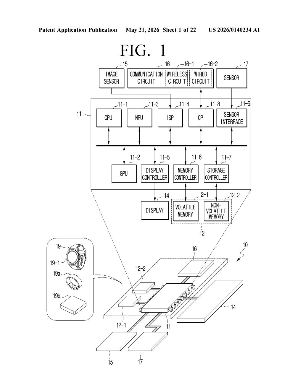
What Samsung's groove-mounted laser sensor actually does
Imagine a health sensor on your wrist that shines several colors of light through your skin simultaneously — some wavelengths are great at tracking blood oxygen, others at heart rate or blood glucose. Right now, building something like that requires carefully aligning separate laser components, which is fiddly, expensive, and hard to miniaturize.
Samsung's patent describes a sensor where a single laser diode gets physically snapped into a carved groove in a chip substrate. Because the groove is machined to exact dimensions, the laser's light-emitting points line up automatically with tiny light guides (waveguides) already built into the chip — no manual alignment needed. The light travels through those guides to output points on the sensor's surface, where it shines into your skin and bounces back for analysis.
A secondary tap on one of those light paths diverts a small sample of the laser's output to an internal detector, so the chip can monitor and regulate the laser's power without any external components. The whole thing is designed to be compact enough to fit inside a wearable or handheld device.
How the waveguide array routes light for biometric reads
The core innovation is a passive self-alignment mechanism. The substrate has a precisely cut groove, and the laser diode sits in it. Because the groove depth is controlled at manufacturing time, the laser's active layer — the strip inside the diode where light is actually generated — ends up at the same height as the waveguides etched into the substrate. No active calibration, no adhesive shimming.
From that laser, multiple wavelengths of light emerge from different emission points along the active layer. Each wavelength couples into its own dedicated waveguide, which then routes the light through a network of first optical lines (think: tiny highways inside the chip) toward light output structures — the points where light exits the chip toward the user's skin.
- First optical lines carry light from waveguides to output structures on the sensor surface
- Second optical lines branch off one of the first lines and redirect a portion of that light inward
- A light detecting element sits on the substrate and reads the tapped signal, enabling real-time power monitoring of the laser
This tap-and-monitor loop (sometimes called a power monitor in photonics) is important because laser output can drift with temperature or age. By sampling light internally, the chip can keep its output stable without needing a separate external feedback sensor.
What this means for next-gen wearable health sensors
Wearable health monitoring — think continuous blood oxygen, pulse, or eventually non-invasive blood glucose — lives or dies on how accurately and how small you can make the light source and detector. Multi-wavelength sensing is more accurate than single-wavelength, but it usually means stacking multiple components. Samsung's self-aligning groove approach could make a multi-wavelength photonic sensor manufacturable at scale without the precision assembly costs that typically come with it.
If this makes it into future Galaxy Watch or Galaxy Ring hardware, you could be wearing a device with lab-grade multi-spectral sensing that's no bigger than what exists today. The internal power monitor also matters for battery life — a sensor that can self-regulate laser output wastes less energy driving a laser harder than it needs to go.
This is solid photonics engineering, not a flashy AI play — but it's exactly the kind of unglamorous substrate-level work that determines whether a wearable health feature is actually useful or just a checkbox on a spec sheet. The self-alignment groove idea is clever and genuinely relevant to Samsung's wearables ambitions. Worth keeping an eye on.
Get our take in your Top Stories
Liked this breakdown? Add Patentlyze as a preferred source on Google, and our plain-English take shows up more often in your Top Stories the next time Samsung patent news breaks.
There are more where this came from
We read every patent application Big Tech publishes and send you the ones worth knowing. Plain English, free, every week.
Want this weekly breakdown for a company we don't cover? Patentlyze Pro →