Samsung Display Patents a Way to Stack Electrodes Inside Each Pixel for More Stable Screens
Samsung Display is patenting a way to stack multiple electrodes inside a single pixel, with protective and insulating layers sandwiched between them — a structural approach that could help screens stay stable and precise at the pixel level.
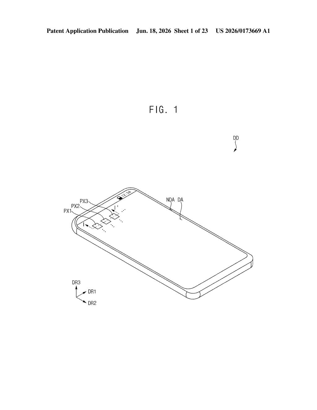
What Samsung's layered pixel electrode design actually does
Think of each pixel on a screen as a tiny light switch. Inside that switch, there are metal contacts that control how much light comes through. Samsung's patent describes a way to build two connected metal contacts stacked on top of each other inside each pixel, with a protective coating and an insulating layer in between.
The idea is that if the bottom contact gets damaged during manufacturing — which happens more than you'd think at microscopic scales — the top contact, sitting above the protective layers, can still carry the electrical signal reliably. You end up with a more fault-tolerant pixel structure.
This same double-layer setup is repeated across neighboring pixel areas, so the pattern works across the whole display. It's a manufacturing and durability play more than a flashy visual feature.
How the stacked electrode and insulating layers fit together
The patent describes a display device with a repeating stacked-electrode architecture inside individual pixel areas on a substrate (the base material a display is built on).
In each pixel area, the structure works like this:
- A first electrode (the bottom contact) sits directly on the substrate.
- A protecting pattern covers part of that electrode — acting like a shield against etching or corrosion during fabrication.
- An insulating pattern then covers both the electrode and the protective layer, electrically separating them from what comes next.
- A second electrode sits on top of the insulating layer, overlapping the first electrode below it, and is electrically connected back to it through a via or opening in the insulating layer.
This entire four-layer sandwich is duplicated for each adjacent pixel area. The key detail is that the top and bottom electrodes in each stack are connected to each other, meaning they function together as a single contact — the stacking isn't about two independent signals, it's about building a more resilient single contact point.
The architecture is well-suited to micro-LED or thin-film transistor displays, where electrode integrity at tiny scales is a known manufacturing challenge.
What this means for future Samsung display panels
Display manufacturing at the microscopic level is full of failure points — a single bad contact in a pixel can mean a dead dot on your screen. By sandwiching a protective layer between two connected electrodes, Samsung's approach gives each pixel a structural backup that could reduce defect rates coming off the production line.
For consumers, the direct benefit would be fewer dead pixels and more consistent brightness across a panel. For Samsung Display — which supplies screens to Apple, among others — better manufacturing yield means lower cost per panel. This is the kind of unglamorous structural patent that quietly shapes what you're looking at every time you open your phone.
This is a manufacturing-layer patent, not a visual experience patent — it won't make colors pop or add a new display mode. But yield improvement and pixel-level reliability are genuinely competitive battlegrounds in the display industry, and Samsung Display files these structural patents with clear intent to defend its process IP. Worth tracking for anyone following OLED or micro-LED supply chains.
Get one Big Tech patent every Sunday
Plain English, intelligent commentary, no hype. Free.
Editorial commentary on a publicly published patent application. Not legal advice.