
Samsung Patents a Screen Design That Makes Each Dot of Light Last Longer
Samsung Display has filed a patent describing a specific internal wiring layout for individual pixels in an OLED screen. It's deep inside the hardware, but this kind of circuit design is what separates good panels from great ones.
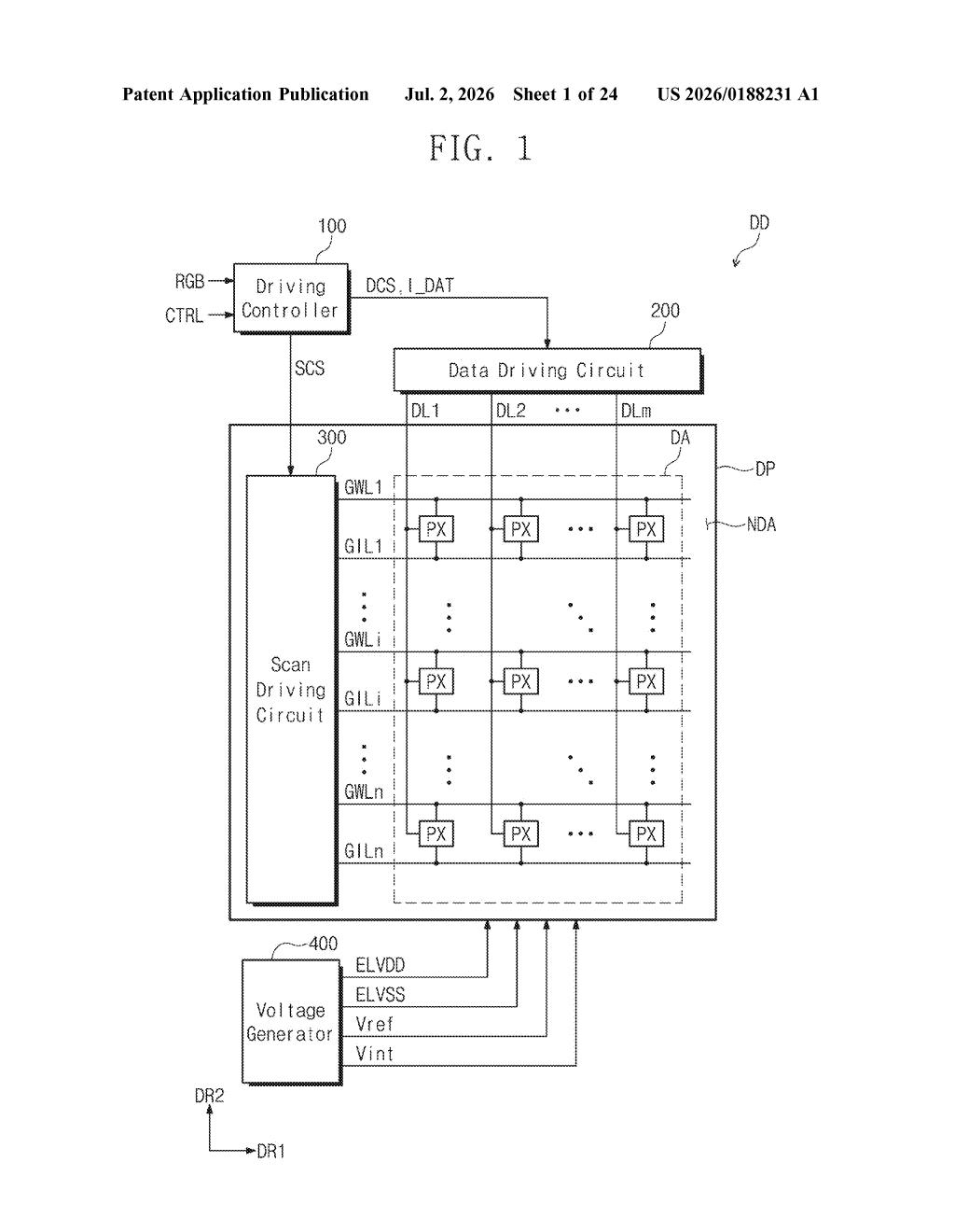
What Samsung's new pixel circuit actually does
Think of each pixel on an OLED screen as its own tiny light switch that needs to turn on and off thousands of times per second with perfect precision. The circuitry behind that switch determines how accurate the color and brightness are, and how efficiently the display uses power.
Samsung Display's patent describes a pixel built around four transistors and a small capacitor. Each transistor plays a specific role: one controls how much current reaches the light-emitting element, one feeds in the image data, one sets a reference level so the pixel knows its "off" baseline, and one resets the pixel between frames. The capacitor holds the voltage steady between those steps.
This kind of design helps prevent the small manufacturing differences between pixels from causing visible unevenness in brightness across a screen. You might know this issue as "mura" on cheaper displays. Getting the circuit architecture right is one of the core ways display makers keep panels looking uniform over time.
How the four-transistor pixel circuit is wired up
The patent covers a pixel circuit for an OLED (organic light-emitting diode) display panel. OLED screens work by running current directly through light-emitting materials rather than backlighting an LCD layer, so the pixel-level circuit that controls that current is critical to image quality.
The described pixel contains four transistors and one storage capacitor arranged in a specific topology:
- First transistor (drive transistor): Sits between the main power line and the light-emitting element's anode (positive terminal). Its gate is at "first node" and it determines how much current flows through the pixel, controlling brightness.
- Second transistor: Connects the data line (which carries the brightness value for a given frame) to the first node. It opens when the first scan signal fires.
- Third transistor: Connects a second node to a reference voltage line. It also responds to the first scan signal, allowing the circuit to sample the drive transistor's threshold voltage (the minimum voltage needed to turn it on) so that variation between transistors can be compensated automatically.
- Fourth transistor: Connects the second node to an initialization voltage line and is triggered by a separate second scan signal. This resets stored charge between frames, preventing ghosting.
- Storage capacitor: Bridges the first and second nodes, holding the programmed voltage stable while the pixel is emitting light.
The two-node, two-scan-signal structure is designed to enable threshold voltage compensation (automatically correcting for transistor-to-transistor manufacturing variation) while keeping the pixel footprint compact.
What this means for future Samsung screens
Pixel circuit architecture is one of the least glamorous but most consequential parts of display engineering. When individual transistors age or vary slightly from manufacturing, pixels drift in brightness, causing visible patches on the screen. A well-designed compensation circuit catches that drift before it reaches your eyes. Samsung Display's approach here uses a relatively compact four-transistor structure, which matters because smaller pixel circuits leave more room for the light-emitting element itself, which can improve brightness and power efficiency.
Samsung Display supplies OLED panels to Samsung's own Galaxy phones and tablets, as well as Apple's iPhones and iPads. Circuit-level improvements like this one work their way into future panel generations, meaning they can affect the display quality of products from multiple brands.
This is a straightforward circuit patent covering fundamental OLED pixel design. It's not the kind of filing that signals a dramatic new product direction, but pixel compensation circuits are genuinely important to panel quality and longevity. If you follow display technology closely, it's worth a note; if you don't, this one is safely skippable.
Get our take in your Top Stories
Liked this breakdown? Add Patentlyze as a preferred source on Google, and our plain-English take shows up more often in your Top Stories the next time Samsung patent news breaks.
There are more where this came from
We read every patent application Big Tech publishes and send you the ones worth knowing. Plain English, free, every week.
Want this weekly breakdown for a company we don't cover? Patentlyze Pro →