
Samsung Patents a Night-Vision Chip That Reads Heat to Capture Images in the Dark
Samsung is patenting a thermal image sensor with a deliberately perforated absorption layer, a structural tweak designed to improve how accurately the sensor captures heat rather than visible light.
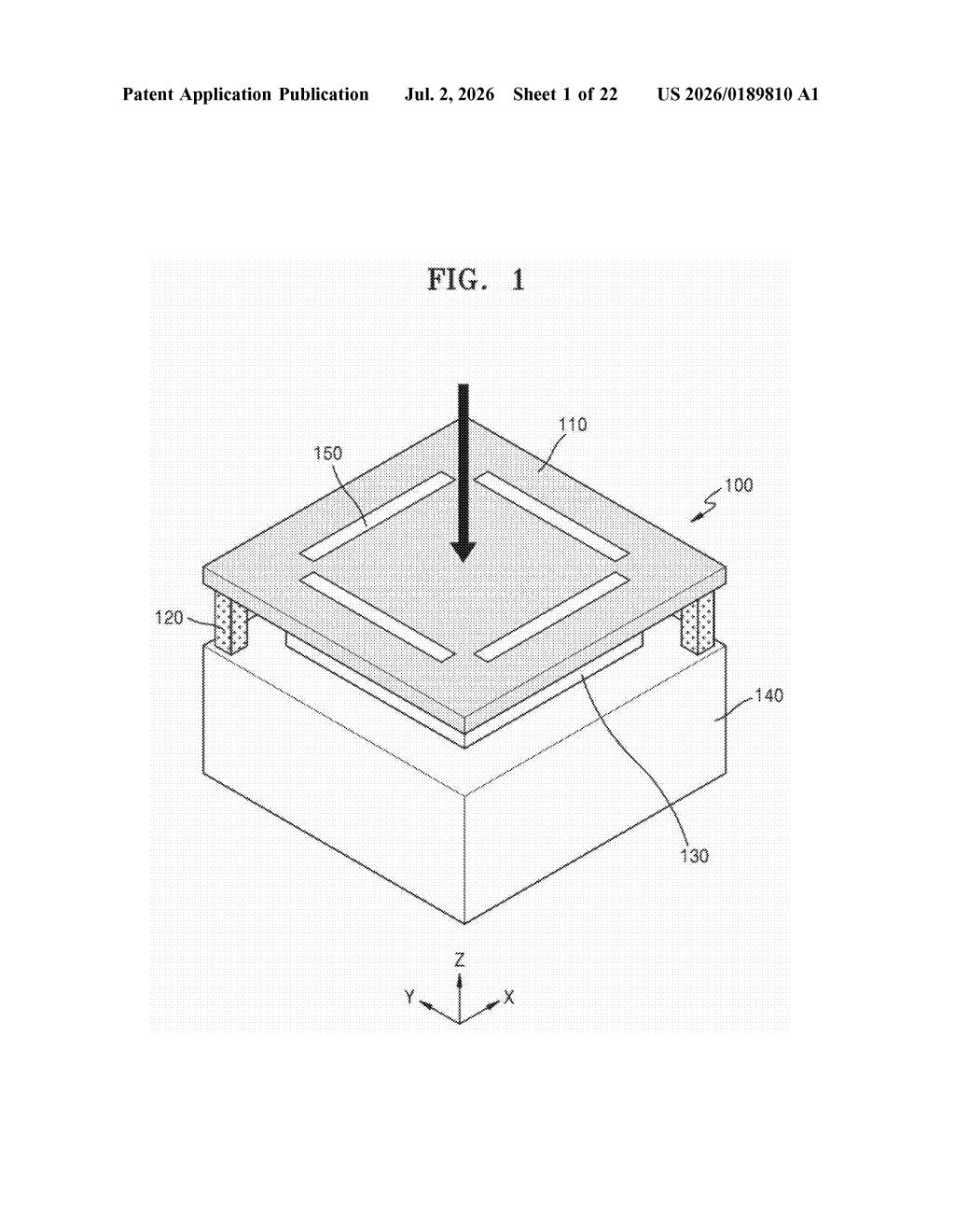
What Samsung's patterned thermal sensor actually does
Thermal cameras don't record color or brightness the way a regular camera does. Instead, they detect heat radiating from objects, turning temperature differences into a visible picture. Your TV remote, a person standing in a dark room, or an overheating circuit board all glow differently in thermal imaging.
The challenge is building a sensor that picks up heat signals cleanly without interference from the sensor's own structure warming up and muddying the reading. Samsung's patent describes a sensor with a special layered design: an absorption layer on top that soaks up infrared heat, sitting above a grid of tiny temperature sensing cells. Critically, holes are punched through the absorption layer in a deliberate pattern, and the gaps between the sensing cells are filled with an insulating material.
Think of the holes as relief valves that prevent unwanted heat from building up across the layer unevenly. The insulating filler keeps each sensing cell isolated from its neighbors, so one hot spot doesn't bleed into the next. The whole assembly floats above the base chip on a support structure, keeping it thermally separated from the electronics below.
How the hole pattern and insulating layer work together
The sensor is built as a composite layer suspended above a substrate (the base chip) by a support structure. That air gap between the sensor layer and the substrate is intentional: it thermally isolates the sensitive parts from the rest of the electronics, which generate their own heat and could otherwise corrupt the readings.
The composite layer has two parts stacked together:
- Absorption layer (top): captures incoming infrared radiation, the kind of heat energy emitted by warm objects
- Sensor array layer (bottom): a grid of individual temperature sensing cells that convert absorbed heat into electrical signals
A pattern of holes is etched through the absorption layer. This patterning controls how heat spreads across the layer and can help tune the sensor's response to specific infrared wavelengths. Without it, the absorption layer could trap and redistribute heat unevenly, reducing measurement precision.
The sensor array layer also includes an insulating material that surrounds each sensing cell and fills the gaps between them. This prevents thermal or electrical crosstalk (where a signal in one cell leaks into a neighboring cell), which is a common source of blur or inaccuracy in dense sensor arrays. The overall architecture aims to sharpen the thermal picture the sensor produces.
What this means for Samsung's future thermal camera hardware
Thermal sensors are increasingly finding their way into consumer electronics, from smartphone cameras used for augmented reality depth sensing to health monitors that track skin temperature without contact. A more accurate, compact thermal sensor could make these features more reliable and cheaper to include in everyday devices.
For Samsung specifically, tighter control over thermal sensor accuracy matters across multiple product lines: Galaxy smartphones, Galaxy wearables, and industrial or security camera hardware the company supplies to other manufacturers. This patent sits at the component level, meaning any improvement here could flow through to a wide range of end products rather than a single device.
This is a materials and microstructure patent, not a headline product announcement. It is genuinely incremental work on sensor architecture, the kind of foundational filing that rarely gets press coverage but matters a lot if you are trying to build a thermal camera thin enough to fit inside a phone. Worth tracking if you follow Samsung's sensor supply business.
Get our take in your Top Stories
Liked this breakdown? Add Patentlyze as a preferred source on Google, and our plain-English take shows up more often in your Top Stories the next time Samsung patent news breaks.
There are more where this came from
We read every patent application Big Tech publishes and send you the ones worth knowing. Plain English, free, every week.
Want this weekly breakdown for a company we don't cover? Patentlyze Pro →