
New Image Sensor Patent Tackles Pixel Interference at the Source
Sony has filed a patent describing a new way to physically separate the light-sensing zones inside an image sensor, a design that could reduce the color bleeding and noise that shows up in photos taken in difficult lighting.
What Sony's pixel separation design actually does
Imagine each pixel in a camera sensor as a tiny plot of land. For a photo to be sharp and accurate, each plot needs good fences: light hitting one pixel shouldn't bleed into its neighbor, and the electrical signals they generate shouldn't interfere with each other.
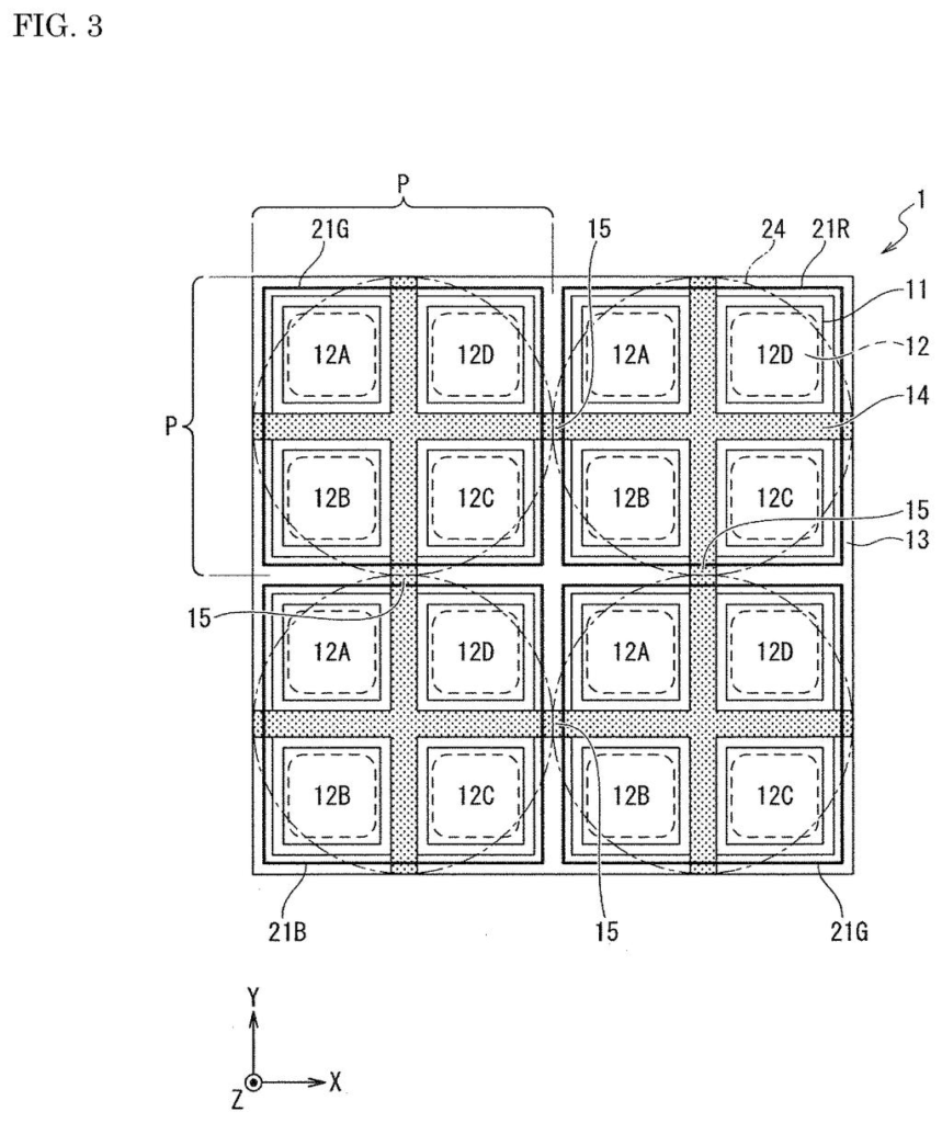
Sony's patent describes a more detailed fencing system. Each pixel is itself divided into several smaller light-catching zones, and Sony wants to place a specific material layer between those inner zones to keep them electrically separated. Then, at the boundary between neighboring pixels, a connecting structure ties those inner fences together, so the whole grid stays consistent across the sensor.
The goal is to improve what engineers call "optical characteristics", basically, how cleanly the sensor captures light. Better separation means less crosstalk (where one pixel's signal leaks into another), which translates to sharper colors and less noise in your photos, especially in low light.
How Sony's connection unit links intra-pixel barriers
The patent describes an image sensor built on a semiconductor substrate with pixels arranged in a grid. Each pixel contains multiple photoelectric conversion units (the tiny zones that turn incoming light into an electrical charge).
There are two types of separation structures at work:
- Inter-pixel separation unit: A barrier with a physical gap that sits between neighboring pixels, blocking both electrical and optical interference from crossing over.
- Intra-pixel separation unit: A material layer inside each pixel that sits between its internal photoelectric conversion zones, keeping their electrical signals distinct from one another.
The novel piece is a connection unit that bridges the intra-pixel separation structures of two adjacent pixels. Rather than having each pixel's internal barriers be isolated islands, this connector ties them together at the pixel boundary, creating a more continuous and structurally stable separation network across the entire sensor surface.
Note: there is a mismatch between this patent's abstract (which describes an image sensor) and its first independent claim (which describes a software method for securing backup storage using virtual air gaps). The summary above is based on the abstract and title, which appear to reflect the actual invention.
What this means for camera image quality
Image sensors are at the heart of every smartphone camera, security camera, and medical imaging device Sony supplies components for. Even small improvements in how cleanly pixels separate their signals can reduce noise and improve color accuracy, particularly in the low-light scenarios where sensors struggle most.
For consumers, this kind of sensor-level refinement is what drives the annual camera improvements you see in flagship phones. Sony supplies image sensors to Apple, Google, and others, so structural patents like this one can have wide downstream reach well beyond Sony's own camera products.
This is solid, unglamorous semiconductor engineering. Pixel separation structures aren't headline material, but they are exactly the kind of incremental improvement that compounds into real-world camera gains over successive sensor generations. Given Sony's dominant position in the image sensor supply chain, any structural refinement it patents is worth tracking.
There are more where this came from
We read every patent application Big Tech publishes and send you the ones worth knowing. Plain English, free, every week.
The drawings
34 drawing sheets from US 2026/0223469 A1 · click any drawing to enlarge


Want this weekly breakdown for a company we don't cover? Patentlyze Pro →
Be the first to weigh in