Sony Patent: Camera Uses AI to Select Which Scene Areas to Capture
Most camera sensors dutifully read every single pixel, every single frame, whether anything interesting is happening or not. Sony's new patent describes a sensor that skips the boring parts, letting an on-chip AI decide which pixels are even worth checking.
What Sony's AI-directed pixel readout actually does
Imagine a security camera that has to scan millions of dots of light every second, even when the scene hasn't changed at all. That's a lot of wasted work, and wasted energy, just to confirm that nothing moved.
Sony's patent describes a smarter approach: a tiny neural network built directly into the image sensor itself. Instead of blindly handing off every pixel to the rest of the system, this AI layer scans an initial pass of the image and figures out which regions actually need a closer look. It then tells the sensor's readout circuitry to focus only on those areas.
The result is a sensor that can prioritize what matters, whether that's a moving object, a face, or a specific zone in the frame, without waiting for a separate processor to weigh in. All the decision-making happens right on the chip, before the data even leaves the sensor.
How the neural network picks which pixels to scan
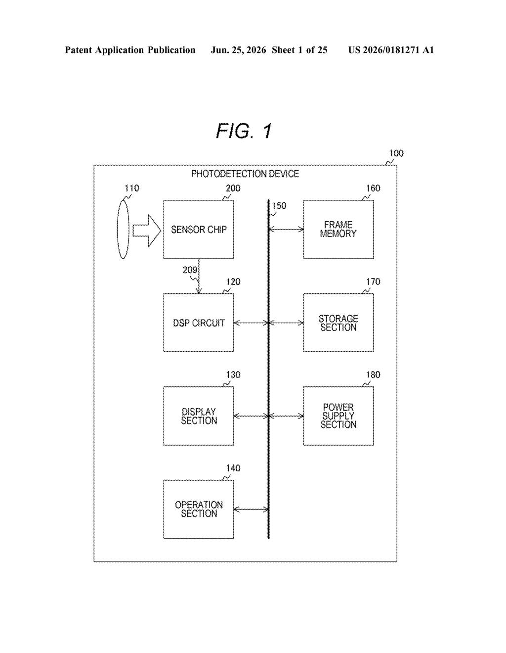
The patent describes a photodetection device built around three linked components working in a tight loop.
First, a pixel array section captures raw light data across the sensor surface, exactly as conventional image sensors do. That raw data (called sensor data in the patent) is fed immediately to a neural network circuit embedded on the same chip. This circuit runs a trained model against the incoming pixel data and produces line data, a structured output that encodes where in the frame something meaningful is occurring.
That line data then flows to a readout control section, which generates a control signal telling the sensor which group of pixels to actually read out in full detail. Pixels in regions flagged as unimportant can be skipped or sampled at lower resolution, while flagged regions get full attention.
- Pixel array: captures raw image data across the sensor
- Neural network circuit: runs inference on that data to identify regions of interest
- Readout control section: uses the inference result to selectively read only the pixels that matter
The key architectural point is that the AI processing sits between the pixel capture and the readout stages, rather than downstream of a full-frame data dump. This is sometimes called in-sensor computing.
What this means for cameras in sensors and devices
For consumer cameras, the gains are mostly about speed and efficiency. A sensor that skips irrelevant pixels can deliver faster effective frame rates on fast-moving subjects, or save battery life in always-on applications like face detection or gesture recognition, without requiring a separate AI accelerator chip.
The broader potential is in specialized sensors: automotive cameras that need to lock onto pedestrians instantly, industrial inspection systems, or medical imaging devices where you want real-time region targeting without a bulky external processor. Sony is one of the world's largest image sensor suppliers, so even a patent at this stage carries weight. If this architecture reaches production, it would move AI inference from a downstream software step to a physical property of the sensor hardware itself.
This is a genuinely interesting architectural move, not a flashy consumer feature but the kind of chip-level design decision that reshapes what cameras can do. Putting the inference step inside the sensor, before the readout, is a different philosophy from the current approach of dumping all the pixels out and sorting them later. Whether Sony actually ships this or it stays a patent is the real question.
Get one Big Tech patent every Sunday
Plain English, intelligent commentary, no hype. Free.
Editorial commentary on a publicly published patent application. Not legal advice.